2.10 VOLTAGE-MULTIPLIER CIRCUITS
160 likes | 449 Vues
Learn about voltage multiplier circuits in electronics, including voltage doubling, tripling, and quadrupling concepts. Explore different configurations and understand their applications in maintaining peak voltages while stepping up output voltages.

2.10 VOLTAGE-MULTIPLIER CIRCUITS
E N D
Presentation Transcript
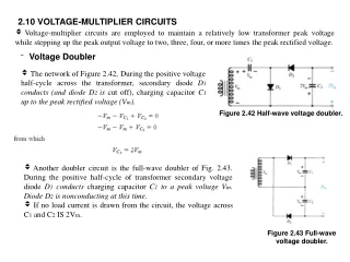
2.10 VOLTAGE-MULTIPLIER CIRCUITS • Voltage-multiplier circuits are employed to maintain a relatively low transformer peak voltage while stepping up the peak output voltage to two, three, four, or more times the peak rectified voltage. • Voltage Doubler • The network of Figure 2.42,During the positive voltage • half-cycle across the transformer, secondary diode D1 conducts (and diode D2 is cut off), charging capacitor C1 up to the peak rectified voltage (Vm). Figure 2.42 Half-wave voltage doubler. • Another doubler circuit is the full-wave doubler of Fig. 2.43. During the positive half-cycle of transformer secondary voltage diode D1 conducts charging capacitor C1 to a peak voltage Vm. Diode D2 is nonconducting at this time. • If no load current is drawn from the circuit, the voltage across C1 and C2 IS 2Vm. Figure 2.43 Full-wave voltage doubler.
Voltage Tripler and Quadrupler • Figure 2.44 shows an extension of the half-wave voltage doubler, which develops three and four times the peak input voltage. In operation capacitor C1 charges through diode D1 to a peak voltage, Vm, during the positive half-cycle of the transformer secondary voltage. Capacitor C2 charges to twice the peak voltage 2Vm developed by the sum of Figure 2.44 Voltage tripler and quadruple • the voltages across capacitor C1 and the transformer, during the negative half-cycle of the transformer secondary voltage. • During the positive half-cycle, diode D3 conducts and the voltage across capacitor C2 charges capacitor C3 to the same 2Vm peak voltage. On the negative halfcycle, diodes D2 and D4 conduct with capacitor C3, charging C4 to 2Vm. • The voltage across capacitor C2 is 2Vm, across C1 and C3 it is 3Vm, and across C2 and C4 it is 4Vm. If additional sections of diode and capacitor are used, each capacitor will be charged to 2Vm. Measuring from the top of the transformer winding (Fig.2.44) will provide odd multiples of Vm at the output, whereas measuring the output voltage from the bottom of the transformer will provide even multiples of the peak voltage, Vm.
2.11 power supply • Introduction: • Starting with an ac voltage, we abtain asteady dc voltage by rectifying the ac voltage, then filtering to a dc level and finally, regulating to obtain a desired fixed dc voltage . • A block diagram containing the parts of atypical power supply is shown in fig.(2. 45). Fig.(2. 45) Block diagram showing parts of power supply.
12.2 GENERAL FILTER CONSIDERATIONS • Before going into the details of a filter circuit, it would be appropriate to consider the usual methods of rating filter circuits so that we can compare a circuit’s effectivenessmas a filter. Figure 2.46 shows a typical filter output voltage, which will be used to define some of the signal factors. The filtered output of Fig. 2.46 has a dc value and some ac variation (ripple). Although a battery has essentially a constant or dc output voltage, the dc voltage derived from an ac source signal by rectifying and filtering will have some ac variation (ripple). The smaller the ac variation with respect to the dc level, the better the filter circuit’s operation. Figure 2.46 Filter voltage waveform showing dc and ripple voltages.
Consider measuring the output voltage of a filter circuit using a dc voltmeter and an ac (rms) voltmeter. The dc voltmeter will read only the average or dc level of the output voltage. The ac (rms) meter will read only the rms value of the ac component of the output voltage (assuming the ac signal is coupled through a capacitor to block out the dc level). Defined as: Ripple is (2 – 28) VOLTAGE REGULATION: is the amount the dc output voltagechanges over a range of circuit operation. (2 – 29)
RIPPLE FACTOR OF RECTIFIED SIGNAL • We will see that the full-wave rectified signal has a larger dc component and less ripple than the half-wave rectified voltage. • In summary, a full-wave rectified signal has less ripple than a half-wave rectified signal and is thus better to apply to a filter. • H.W.R: Vodc = 0.318 Vm • Vr(rms) = 0.385 Vm • H.W.R: Vodc = 0.636 Vm • Vr(rms) = 0.308 Vm r = Vr(rms)/ Vdc * 100% = 0.385 Vm / 0.318 Vm * 100% = 121% r = Vr(rms)/ Vdc * 100% = 0.308Vm / 0.636 Vm * 100% = 48% 12.3 CAPACITOR FILTER Simple capacitor filter.
Figure 2.47 Capacitor filter operation: (a) full-wave rectifier voltage; (b) filtered output voltage. Figure 2.47a shows the output voltage of a full-wave bridge rectifier before the signal is filtered. Whereas 2.47b shows the resultig waveform after the filter capacitor is connected at the rectifier output. Notice the filtered waveform is essentially a dc voltage with some ripple (for ac variation). Fig.(2.47b) shows the waveform across a capacitor filter. Time T1 is the time during which diodes of a full – wave rectifierconduct, charging the capacitor up to the peak rectifier voltage Vm. Time T2 is the time interval during which the rectifier voltage drops below the peak voltage, and the capacitor discharges through the load.
RIPPLE VOLTAGE, Vr(rms): • Assuming triangle ripple waveform: During capacitor discharge, the voltage change across Crs: Approximate the ripple wave to asawtooth signal gives: So and f of F.W.R = 2fH.W.R And ripple factor r = Vr(rms)/ Vdc * 100% =
Diode Conduction Period and Peak Diode Current: • From the previous discussion, it should be clear that larger values of capacitance provide less ripple and higher average voltage, thereby providing better filter action. • Recall that the diodes conduct during period T1 (see Fig. 2.48), during which time the diode must provide the necessary average current to charge the capacitor. Figure 2.48 Capacitor filter: (a) capacitor filter circuit; (b) output voltage waveform.
The shorter this time interval, the larger the amount of the charging current. Figure 2.49 shows this relation for a half-wave rectified signal (it would be the same basic oper-ation for full-wave). Notice that for smaller values of capacitor, with T1 larger, the peak diode current is less than for larger values of filter capacitor. Figure 2.48 Output voltageand diode current waveforms: (a) small C; (b) large C.
Since the average current drawn from the supply must equal the average diode current during the charging period, the following relation can be used (assuming constant diode current during charge time): • The charging period, or we can say: • Qdischarge = Qcharge (Q: charge of capacitor) ( 2 – 30) 12.4 RC FILTER: • It is possible to further reduce the amount of ripple across a filter capacitor by using an additional RC filter section as shown in Fig. 19.8. The purpose of the added RC section is to pass most of the dc component while attenuating (reducing) as much of Figure 2.49 RC filter stage.
The ac component as possible. Figure 2.50 shows a full-wave rectifier with capacitor filter followed by an RC filter section. The operation of the filter circuit can be analyzed using superposition for the dc and ac components of signal. Figure 2.50 Full-wave rectifier and RC filter circuit.
(2 – 41) (2 – 42) As C is large in µF, f = 100Hz so XC ≈ XC2 //RL for C= 100µF and XC ˂˂R XC = 1/2лfc = 1/ 2л* 0.0001*100 = 100/ 2л = 15.9 Ω Finally how to get a power supply circuit using zener diode of Vz=6V.
Fig. 2.49 • And we can use IC voltage regulator, such as three terminal voltage regulator such as the series 78 regulators. Figure 2.50 5-V power supply.