
Pacific Nanotechnology
E N D
Presentation Transcript
Presentation Outline • Introduction to Probe Microscopy • Nanotechnology Applications • PNI Products
What is an SPM • An SPM is a mechanical imaging instrument in which a small, < 1 µm, probe is scanned over a surface. By monitoring the motion of the probe, the surface topography and/or images of surface physical properties are measured with an SPM. z y z
Revolutionary Capabilities • Sensitivity independent of size • Built in at the atomic scale • Making bigger does not make more sensitive • Machine forming technology • From 1 micron to .1 nm • Motion control technology • Nano scale motion control • Manufacturing techniques
Profilers In 1929, Smaltz described a tracer instrument using a tilting mirror and a long light arm to obtain the necessary magnification.
Profilers - 1955 - Vibrating tip profiler - From null point to surface - Piezo activated Motion - Piezo detection of surface Becker U.S. #2,728,222
TopoGraphiner - 1972 - Non-contact profiler - X,Y,Z Piezo - Constant current feedback
Scanning Tunnelling Microscope - 1982 - Needle Close to Surface - Reduce Vibrations - x,y,z Piezoelectrics/Feedback Pictures of Atoms !!!
SPM Timeline 2000 1900 • 1929 – Optical Profiler with 25 nm resolution • 1955 – Vibration profiler with piezoelectrics • 1972 – Topographiner – non contact profiler • 1982 – Scanning Tunneling Microscope – Atomic resolution • 1986 – Atomic Force Microscope – Insulating materials • 1990-2000 – Drastic expansion of techniques (modes, lithography)
Why AFM ? • Unique Combination of Characteristics • 3-D Magnification: X-Y, and Z • All Environments: Air, Liquid, Vacuum • Proximal Probes: Surface Physical Properties
A Family of Microscopes SPM (air, liquid, vacuum) STM Topography Spectroscopy Lithography EChem. BEEM AFM Contact Modes Topography LFM, SThM Lithography AC Modes Topography MFM, EFM SKPM Others SNOM(NSOM) Aperture Aperatureless Reflection Transmission EChem
SEM Comparison SEM AFM Wide range of sample roughness True 3D image Operated in low to high vacuum Vacuum, Air or Liquid
AFM Stage Z Motion Control Optic xyz scanner AFM Force Sensor XY Motion Control
AFM Light Lever – Force Sensor Signal out Differential Amplifier Sample When the cantilever moves up and down, the position of the laser on the photo detector moves up and down.
Materials Science Food Health Care Transportation InformationTechnology Construction Military Consumer Materials SciencesFundamental Research Materials Science encompasses the study of the structure and properties of any material, as well as using this body of knowledge to create new types of materials, and to tailor the properties of a material for specific uses. The field encompasses the spectrum of materials: metals, ceramics, polymers (plastics), semiconductors, and combinations of materials called composites"
Fundamental Understanding the Properties of Materials at the NanoScale. • NanoStructuresNanoTubesNanoWiresNanoCrystalsNanoParticles • NanoLithography • NanoMechanics • Materials CeramicsPolymers
Carbon NanoTubes Single Wall NanoTubes Physical Properties Mechanics Electrical Thermal Bulk Properties Composites MultiWall Nanoteubes
NanoElectronics 30 nm NanoWire Molecular Electronics Quantum Computers Optical Devices 30 nm Diameter Quantum Dots
NanoCrystals CaP21 X 21 µ Polymer Crystal24 X 24 µµ SrTiO3 X 3 µ
NanoMechanics Hong LiangUniv. of Alaska Fairbanks
Polymers Topography 1.4 X 1.4 µ Material Sensing – Phase SBS Copolymer
NanoParticles • Surface/Volume Ratio Increases • New Physical Properties • Engineered • Pharmaceuticals • Performance Chemicals • Cosmetics • Non – Engineered • Environmental • Controlled Ambient
NanoParticles Scan of colloidal gold and associated particle size distribution. Mean Ш = 28nm.
AFM - NanoParticles • Qualitative • 3D Visualization • Material Sensing • Quantitative • Size • Morphology • Surface Texture/Roughness • Statistical information – Counting, Size Distribution, Volume/Mass Distribution
AFM NanoLithography • NanoScale Surface Modifications • Mechanical/Electrical/Chemical • Resolution Depends on Probe Diameter
Anodic Oxidation 2x 3x 1x 50nm 150nm 100nm Pattern writing using accurate position sensors
Charge Lithography PZT material modified by electric stimulus
Chemical Lithography Lines written by depositing chemicals on a surface. ODT on Gold. Peter Schwartz, Cal Poly San Luis Obispo
Commercial NanoTechnology • High Resolution Microscopy is essential for developing new products. • Materials science fundamental research is now being applied in several sectors. • Often the applications are tied to the understanding of old processes.
Health Care - BioSensors Plasma DNA1.5 X 1.5 µ Straightened DNA~1 X 1 µ
Transportation - Metallurgy 95 X 95 µ 23 X 23 µ NiAl, 26 at% Al dendrite structure Optical Microscope Image
Consumer - Paper AFM is used to understand the glossing characteristics of paper surfaces 100 X 100µ
Consumer - Tires Carbon black, commonly used to enhance the properties of manufactured rubber 2 X 2 µ
Consumer – Razor Blade Cutting edge of razor blade 4 X 4 µ
Consumer – Plastic bags Extruded polyethylene, commonly used in manufacturing great variety of consumer products, Blending with NanoParticles gives new properties. 35 X 35 µ
Applications Summary • AFM • High Resolution, 3-D • Nano Applications • Fundamental • Commercial
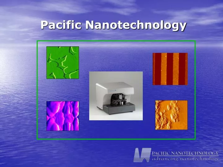
PNI Products • Nano-R™ SPM System • Nano-I™ System • Image Analysis Products • AFM Probes
Nano-R™ Stage High Resolution Video Microscope Scanner Light LeverCrystal Sample Puck X-Y Stage(in granite block)
Nano-R™ SPM System High Performance Easy To Use Versatile
High Performance • High Resolution Optics • XYZ Calibration Sensors • Stable Stage Design
High Resolution Video Microscope Optical Microscope Software control of videomicroscope functions
Video Optical Microscope Laser AlignmentFeature Location
X-Y-Z Calibration Sensors Superior Zoom to Feature Linearity Correction Calibration in X-Y-Z
Zoom to Feature Zoom Step 1
Calibration & Linearity VLSI Pitch Standard 3.06µ+/-1% Pitch 1: 3.049µPitch 2: 3.084µ
Low Noise Terraces on SrTiO measured with the Nano-R™ LL-AFM 0.328 nm
Easy to Use • Motorized XY Stage • Probe Exchange