Download
1 / 8
80 likes | 184 Vues
Since 1992, our semiconductor lab in Munich develops cutting-edge silicon detectors. We specialize in thinning sensors and bump bonding technologies for various projects. Seeking industry partners for mass production.

E N D
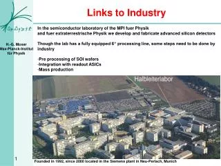
Links to Industry • In the semiconductor laboratory of the MPI fuer Physik • and fuer extraterrestrische Physik we develop and fabricate advanced silicon detectors • Though the lab has a fully equipped 6“ processing line, some steps need to be done by industry • Pre processing of SOI wafers • Integration with readout ASICs • Mass production 1 Founded in 1992, since 2000 located in the Siemens plant in Neu-Perlach, Munich
HLL Facilities 800m² cleanroom Class 1 6“ productionline Thermal oxidation Photolithography (double sided, maskandlaserwriter) Wetchemicalething Ion implantation LTO Nitride Polysilicon Al-sputtering
Products and Projects • Strip and Pixel Detectors (ATLAS SCT and Pixel) • Silicon Drift Chambers • pn-CCD (fully depleted) (XMM-Newton, eRosita) • Silicon Photomultipliers • Thin Pixel detectors + 3D Integration (sLHC, rad hard) • DEPFET Active Pixel Detectors for x-ray imaging and tracking (Belle II)
Need For Thin Silicon n p+ • Thin pixel sensors for ATLAS • Good CCE after irradiation • Less material • Thickness: 75 – 150 µm n-depleted gapregion n-non-depletedregion n-non-depletedregion • Thin DEPFET active pixel sensors for Belle II (and ILC) • Low multiple scattering • Belle II < 0.19% X0 n+ Cut through the matrix • SiMPl SiPMs with bulk integrated quench resistors • Simple processing • Ideal for 3D integration • Need tuning of pitch, bulk resistivity and thickness • => Thin silicon ~ 50 µm 450mm 50mm 4
Sensor Thinning ? Need thin (50µm-75µm) self supporting all silicon module Process backside e.g. structured implant etching of handle wafer (structured) Thinning of top wafer (CMP) Processing diodes and large mechanical samples Belle II module Wafer bonding SOI process
SOI bonding done in industry • Highly non standard! • Wafers need to be prepared (implanted) by us • Rather thick wafer (CMOS SOI ~ nm!, more like MEMS) • Bonding of wafers with structured implants not trivial • Need high quality (clean, polishing, MEMs not ok) • Only few companies can do it and even less are willing to do this • Similar product needed by CNM, Barcelona 6 etching of handle wafer (structured) Thinning of top wafer (CMP) Processing Wafer bonding SOI process
Bump Bonding Preparation • Flip chip bump bonding becomes more end more important for pixel sensors • Large pitch bumping (~200 µm) • auxiliary ASICs for active pixel sensors (DEPFETs) • large pixel (pad) detectors (x-ray imaging) • bumping of ASICs done by industry (C4) • (ASIC fab, cheap)) • needed: UBM for sensor + flip chip • 2) Medium pitch (~50 µm) • bumping not yet standard (some specialists, expensive) • 3) Fine pitch ( < 50 µm) • need for R&D • future: 3D integration IBM C4 solder bumps Pitch: 200 µm Available in MPW ATLAS FEI3 pixel chips with bumps by IZM, Berlin Pitch: 50 µm, wafer level processing Switcher DCD/DHP Flex
Summary • The MPI semiconductor laboratory has interest (and needs) contacts to industry for • SOI wafer preparation • Interconnection (UBM, bumping, flip chip) • Our production capacity is limited to ~100 wafers/year • ok for Belle II, IBL, …. • not ok for large detectors (ATLAS pixel, SiPMs for calorimeter) • Need partners for mass production • Technology transfere (compatibility) • Licence • The MPI semiconductor laboratory offers possiblities to develop and produce novel types of silicon detectors • Could be a partener for other HEP institutes • (needs common research interest, however) 8