Download
1 / 21
220 likes | 362 Vues
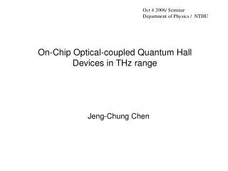
This seminar presented by Jeng-Chung Chen at NTHU explores the innovative on-chip optical-coupled quantum Hall (QH) devices designed for terahertz (THz) applications. It delves into the study of single-electron transistors (SETs) and their characterization, highlighting the excited electronic states in closed quantum dots (QDs). The discussion encompasses device design, passive THz scanning microscopes, and future perspectives on these devices. The findings reveal insights into electron dynamics, tunneling barriers, and the unique behaviors of QDs under varying gating conditions.

E N D
Oct 4 2006/ Seminar Department of Physics / NTHU On-Chip Optical-coupled Quantum Hall Devices in THz range Jeng-Chung Chen
Outline • The study of Single-electron transistor • Device characterization • Excited electronic states in closed QD • Discussion • Conclusion • On-chip optical-coupled QH devices • Passive THz scanning microscopes • Emitter: Hot spots • Detector QH detector • Device design • Future perspective
Single Electron Transistor - Introduction SEM picture 100nm Lateral Confinement Technique Capacitive Charging Model Shadow Evaporation Technique Eg. diameter ~ 0.5-0.2m Cg ~100-10 aF C ~2-0.9 fF Al
Device Characterization Lithographic size of QD : 570nm560nm Temperature: 70-100mK (a)
Qualitative Discussion F0 V1=-1.18V
Discussion: Emperical Model V1=-1.18V fixed In closed QD, regime 2-6
Quantitative discussion U1 U2 UQD Cc~58.8aF, C1sg2=3.12aF
Conclusion – First part • Kinetics of charging and discharging of closed quantum dots (QD)in a GaAs/AlGaAs heterostructure crystal are studied by anAluminum single electron transistor (Al-SET) electrostaticallycoupled to the quantum dot. • The period and conductance of CB peaksof Al-SET associated with different gating conditions revealseveral distinct regimes, strongly depending on the tunnelingbarriers of QD. • A lift-up and an uncovered sinking electronexcited state with long life time are realized in the completelyclosed dot. • An empirical model is proposed to explain the physicalorigins of these transitions. Ref: J.C. Chen, et al. Phys. Rev. B, 74, 045321 (2006).
optics electronics THz microwaves visible x-ray g -ray MF, HF, VHF, UHF, SHF, EHF 0.3–30THz Hz 100 103 106 109 1015 1018 1021 1024 1012 kilo mega giga tera peta exa zetta yotta • 1 THz ~ 1 ps ~ 300 µm ~ 33 cm-1 ~ 4.1 meV Molecular vibration/rotation, Energy levels of quantum structures, magnetic resonance, collective excitations, transit times in mesoscopic devices, superconductor gaps… Biology, chemistry, medics, physics, astronomy, homeland security, environmental monitoring, non-destructive industrial testing, agriculture, …
Picometrix Skin cancer TeraView Detection of chemical drugs Non-destructive check of IC Many applications extensivelydiscussed &studied Mapping of pharmaceutical tablets Security Airport control Medical diagnostics Science (2002)
THz Imaging and Sensing Identification/characterization of the objects Conventional approach Object THz detection External light source THz, NIR, Visible Scattered, Reflected Transmitted P = nW-W Example: Daniel M. Mittleman et. al. IEEE Journal of Selected Topics in Quantum Electronics, 2, 679 (1996).
THz Imaging and Sensing Our approach : Passive / noninvasive Object • Specific dynamics • of the object ? • Activity in • natural state ? THz Detection emitted P = 0.01fW-pW Example: Hall-bar emitter Temp: 4.2K, =2, I=100A, CE: 100pW Ref: K. Ikushima et al., Phys. Rev. Lett. 93, 146804(2004)
μS - - - - - - μS N=3 - + S D N=2 μD μD + + + + + + N=1 U(r) U(r) ● B Δ μSD > ħωc /2 +ΔSD/2 S ΔU(r) D -ΔSD/2 Emitter: Hot spots in IQHE GaAs / AlGaAs heterostructure ħc = 10 meV Classical equi-potential lines in QH states • Higher LLs are fed with electrons via tunneling. Ref: Y.Kawano et al., Phys. Rev. B, 59, p.12537(1999)
k= 2 cm-1 400μm 400 μm Detectors f =13 THz, ε= 10 meV, λ = 100μm, k = 100 cm-1 Detectors Sensitivity (NEP) Speed Narrowband Tunability Quantum Hall (QH)10-15 W/Hz1/2 1ms (Cyclotron resonance, GaAs/AlGaAs 2DEG) Y.Kawano et al., JAP, 89, 4037 (2001) H. Sakuma et al., Far-infrared Phys. & Technol., (2006) Kawano et.al., J. Appl. Phys 89 4037(2001)
On-chip otical coupled quantum Hall devices Ohmic contacts Device design Temp: ~4.2K B_field: ~6-7T Optical consideration 2DEG Light propagation Absorption issue
Study subjects Reference: Ref. C. Wood et al. Appl. Phys. Lett. 88,142103(2006) Organic polymer: benzocyclobutene (BCB) 4mm 1. Application: On-chip THz wave propagation (wave-guide design / switching rate) 2. Physics: (1) Onset of CE in IQHE (2) Temperature dependence (3) FQHE ??
Biological activities Bio-molecules Bio-cell H.Fujitani et al.,J. Chem. Phys. (2005) • Cell thermometry • Molecular “fingerprint” emission activated by ATP hydrolysis Electron dynamics in semiconductors & metals • Landau levels • Size quantization • (QD, 2D-subband) • Impurity levels • Superconductor -gaps • etc.
Future studies Limitation: low temperature ! e.g. QPC in high magnetic field Molecular CNT….etc. Objects Wave guide / antenna design THz photon detector Narrow band /Tunability e.g. Hall bar detector QD / Al-SET detector SIS detectors or mixers CNT….etc.
Lowest: QD Highest: QHm Detected: Pdetect = 0.01aW 0.1pW Emission only from the focal point (10%) Efficiency of optical system (5%) Quantum efficiency of detector (5%) Total emitted: Ptotal CE = 100 aW 100 pW Energy conversion efficiency: 10-7 Electrical: P= RI 2= 3 nW 5 mW I = 500nA 400 μA Detector 10-4 - + e- 10-7 QH device I Intensity of CE