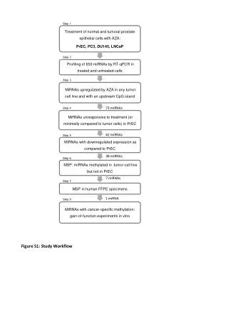
Step 1
a. Step 1. O. Ga. As. In. Model Target Surface: Shown here is GaAs(001)- b 2(2x4). Fully relax surface, test for k-point and plane wave convergence. Then calculate the local density of states (LDOS) to ensure proper band gap width.

Step 1
E N D
Presentation Transcript
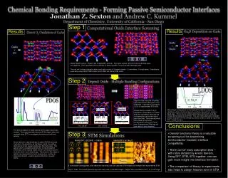
a Step 1 O Ga As In Model Target Surface: Shown here is GaAs(001)-b2(2x4). Fully relax surface, test for k-point and plane wave convergence. Then calculate the local density of states (LDOS) to ensure proper band gap width. The unit cell is show outlined in white, each cell consists of 3 arsenic dimers – 2 row dimers, 1 trough dimer. Calculations were done using VASP, PW91-GGA, 4x2x1 MP K-pts, 400 eV PW cutoff. a Step 2 In2O Clean Density w/ Ga2O Deposit oxide molecule of interest: Calculate several adsorptions from STM data. Calculate and compare LDOS to experimental STS dI/dV. Shown here is a series of In2O adsorption configurations on GaAs. Both the calculated LDOS and the exothermicities are shown below each structure. The conclusion with this system is that some configurations will pin the Fermi level. Experimental STM data will give ratios of sites observed. a a a Ef a Step 3 GaAs(001)-b2(2x4) – Clean GaAs(001) w/ Ga2O eV eV Expt. Experiment Theory Theory If a candidate oxide appears to be stable and unpinned, one can calculate STM images and compare with experimental STM. Ga2O / GaAs: The Tersoff-Hamman approach was used to calculate images. Images were simulated in the -1 to -2 volt range. Results a Results a GaAs + Ga2O GaAs + 2O Volts When Ga2O is Deposited on the GaAs(001)-b2(2x4) surface, the resulting surface structures leave the surface unpinned (no states in band-gap). This is due to surface atoms being restored to bulk-like charge and bonding environment. This sub-oxide passivation template allows for growth of thick-amorphous metal oxides to make an unpinned III/V –Oxide interface Total DOS Ef Volts Conclusions a DH= -2.5 eV DH= -3.5 eV The direct oxidation of GaAs-b2(2x4) with oxygen atoms was studied. The experimentally observed STM oxygen sites were modeled using DFT to investigate the nature of fermi level pinning. Shown above is a partial density of states (PDOS) per atom. Contrary to the prediction by the Spicer model, the gallium atom bound to two oxygen atoms pins the Fermi-level. This gallium atom is charged positively due to electronegative withdrawal, which causes states from the conduction band to be drawn down into the band-gap. These atomic-like states in gallium are responsible for fermi-level pinning, contrary to previously thought – excess arsenic anti-sites or oxygen atoms. • Density functional theory is a valuable screening tool for determining semiconductor-insulator interface compatibility. • There can be many adsorption sites – with ratios dictated by kinetic barriers. Using DFT, STM, STS together, one can gain much insight into interface formation. • The comparison of theory to experiments also helps to assign features seen in STM O Ga As