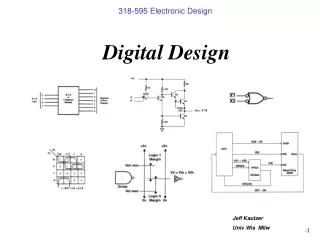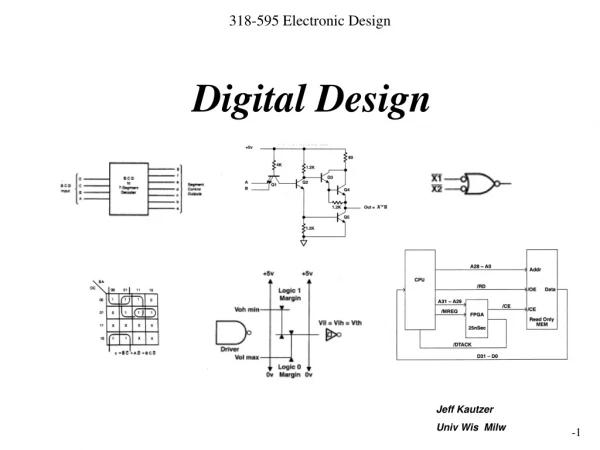
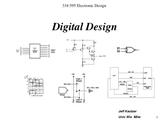
Digital Design
Digital Design. Jeff Kautzer Univ Wis Milw. Programmable Logic. PLD: Programmable Logic Device Typically has defined routing and deterministic function delays. Smaller and less complex than other forms FPGA: Field Programmable Gate Array

Digital Design
E N D
Presentation Transcript
Digital Design Jeff Kautzer Univ Wis Milw
Programmable Logic • PLD: Programmable Logic Device • Typically has defined routing and deterministic function delays. • Smaller and less complex than other forms • FPGA: Field Programmable Gate Array • Routing and ultimate function delay is part of the design process • Complex array of central logic block functions and peripheral I/O functions amidst block-block routing resource • Embedded functions available such as CPU’s (Ex. Altera NIOS)
Comparison of PROM Architecture (Fixed AND, Programmable OR) Programmed PROM Architecture Blank PROM Architecture
Simple FPGA Architecture (Central Logic Block Array, Peripheral I/O Blocks) Routing Resource
Inside the Conf Logic Block Virtex II Series Facts: 1: Each FPGA capable of having 11668 CLB 2: Each CLB has 4 Slices 3: Each Slice - 2 Functional Generators - Arithmetic Login Block - Large Multiplexers - Fast carry look ahead chain - Horizontal chain of OR gates 4: Functioning at 420MHz 5: 3Mb RAM 6: 12 Digital Clock Managers
Different HDL Options Verilog C like syntex. Built-in types and logic representations. Design is composed of modules (functions). Much easier to learn. More cumbersome test bench design. VHDL ADA like syntex and lots of redundancy (can provide more flexibility) Design is composed of entities and are different for different architectures. Harder to learn and complex. Much stronger test bench design.
VHDL BasicsVery High Speed Integrated Circuit (VHSIC) Hardware Description LanguageIEEE Std 1076.1 (VHDL87 & VHDL93)Required by DOD for all ASIC designs • Designs are generally captured in modules which have 2 parts; • Entity Description - Blackbox description including all inputs • and outputs • Architecture Description - Describes the internal signals and • overall relationship of entity inputs to outputs • Best learned by studying examples and not formal language rules
Example - 8 bit comparatorVHDL keywords and library options are in boldComments follow “--” 8 x z 8 y library ieee; -- 1 Use IEEE standard library useieee.std_logic_1164.all; -- 2 Use IEEE standard data type entity jeff is -- 3 entity description, black box name is “jeff” port (x, y: instd_logic_vector (7 downto 0); -- 4 input pin description, 2 eight bit variables, x & y z: out std_logic); -- 5 output pin z, single bit end jeff; -- 6 end of entity description architecture john of jeff is -- 7 separate name for architecture is “john” begin -- 8 keyword z <= ‘1’ when x = y else ‘0’; -- 9 z is “assigned” the value 1 if x = y, else z = 0 end john; -- 10 end of architecture
mux0 mux1 zout mux2 mux3 2 ssel Example - 4:1 MultiplexerVHDL keywords and library options are in boldComments follow “--”
Example - 4:1 MultiplexerVHDL keywords and library options are in boldComments follow “--” library ieee; -- 1 Use IEEE standard library useieee.std_logic_1164.all; -- 2 Use IEEE standard data type entity jeffs_mux is port -- 3 entity description, black box name is “jeffs_mux” (mux0, mux1, mux2, mux3: instd_logic; -- 4 input pin description, Four input signals, mux0-3 ssel: instd_logic_vector (1 downto 0); -- 5 input pin description, 2 bit selection signal “ssel” zout: out std_logic); -- 6 output pin zout, single bit end jeffs_mux; -- 7 end of entity description architecture jeffs_mux of jeffs_mux is -- 8 can have same name for entity and architectures begin -- 9 keyword with ssel select zout <= -- 10 VHDL construct called “with, select, when” mux0 when “00”, -- 11 select mux0 with ssel = 00 mux0 when “01”, -- 12 select mux1 with ssel = 01 mux0 when “10”, -- 13 select mux2 with ssel = 10 mux0 when others; -- 14 select mux3 with ssel = 11 or all other possible end jeffs_mux; -- 15 end of architecture description
mux0 mux1 zout mux2 mux3 2 ssel Example - 4:1 MultiplexerVHDL keywords and library options are in boldComments follow “--” library ieee; -- 1 Use IEEE standard library useieee.std_logic_1164.all; -- 2 Use IEEE standard data type entity jeffs_mux is port -- 3 entity description, black box name is “jeffs_mux” (mux0, mux1, mux2, mux3: instd_logic; -- 4 input pin description, Four input signals, mux0-3 ssel: instd_logic_vector (1 downto 0); -- 5 input pin description, 2 bit selection signal “ssel” zout: out std_logic); -- 6 output pin zout, single bit end jeffs_mux; -- 7 end of entity description architecture jeffs_mux of jeffs_mux is -- 8 can have same name for entity and architectures begin -- 9 keyword with ssel select zout <= -- 10 VHDL construct called “with, select, when” mux0 when “00”, -- 11 select mux0 with ssel = 00 mux0 when “01”, -- 12 select mux1 with ssel = 01 mux0 when “10”, -- 13 select mux2 with ssel = 10 mux0 when others; -- 14 select mux3 with ssel = 11 or all other possible end jeffs_mux; -- 15 end of architecture description • Single quotes used when describing the value assignment to a std_logic type variable • Double quotes used when describing the value assignment to a std_logic_vector type variable • The IEEE std_logic type specifies 9 (nine) possible values including ‘0’, ‘1’, ‘Z’ (high impedance), ‘-’ (don’t care) • among others (not discussed in this basic intro) • Each bit therefore has 9 possible values, A 2 “bit” variable actually has 29 = 81 possible states • “with-select-when” construct useful only if one signal is assigned based on values of input. Another construct called • “case-when” inside of a process statement can be used if more than one signal needs assignment.
4 data x 4 D Latch q aclk reset Example - 4 bit D type latchVHDL keywords and library options are in boldComments follow “--”
Example - 4 bit D type latchVHDL keywords and library options are in boldComments follow “--” library ieee; -- 1 Use IEEE standard library useieee.std_logic_1164.all; -- 2 Use IEEE standard data type entity jeffs_flop is port -- 3 entity description, black box name is “jeffs_flop” (aclk, reset: instd_logic; -- 4 input pin description, clock and reset pins data: instd_logic_vector (3 downto 0); -- 5 input pin description, 4 D type inputs q: out std_logic_vector (3 downto 0)); -- 6 output pin description, 4 latch outputs, q3 - q0 end jeffs_flop; -- 7 end of entity description architecture jeffs_flop of jeffs_flop is -- 8 can have same name for entity and architectures begin -- 9 keyword p1: process (aclk, reset) begin -- 10 VHDL process construct called “if-then” if reset = ‘0’ then q <= (others => ‘0’); -- 11 q is assigned ‘0’ when reset = 0 if rising_edge (aclk) then q <= data; -- 12 q is assigned ‘data” when, reset = 1 and clocked end if; -- 13 end of “if” cases end process; -- 14 end of VHDL case-when end jeffs_flop; -- 15 end of architecture description
4 data x 4 D Latch q aclk reset Example - 4 bit D type latchVHDL keywords and library options are in boldComments follow “--” library ieee; -- 1 Use IEEE standard library useieee.std_logic_1164.all; -- 2 Use IEEE standard data type entity jeffs_flop is port -- 3 entity description, black box name is “jeffs_flop” (aclk, reset: instd_logic; -- 4 input pin description, clock and reset pins data: instd_logic_vector (3 downto 0); -- 5 input pin description, 4 D type inputs q: out std_logic_vector (3 downto 0)); -- 6 output pin description, 4 latch outputs, q3 - q0 end jeffs_flop; -- 7 end of entity description architecture jeffs_flop of jeffs_flop is -- 8 can have same name for entity and architectures begin -- 9 keyword p1: process (aclk, reset) begin -- 10 VHDL process construct called “if-then” if reset = ‘0’ then q <= (others => ‘0’); -- 11 q is assigned ‘0’ when reset = 0 if rising_edge (aclk) then q <= data; -- 12 q is assigned ‘data” when, reset = 1 and clocked end if; -- 13 end of “if” cases end process; -- 14 end of VHDL case-when end jeffs_flop; -- 15 end of architecture description • VHDL Process construct used to embody an algorithm, starts with a label, “p1” • Process contains “sensitivity” list which contains all signals that can possible cause the value of output q to change • The process can be thought of an algorithm although the implication is that all cases are evaluated concurrently because • the implementation is in hardware and not software! • The signal “data” is not in the sensitivity list because it can change at any time and does directly effect the output, q
Example - State MachineBus Arbitor req0 * /req1 ack0 gnt0=0 gnt1=1 ack1 gnt0=1 gnt1=0 /req0 * req1 /req0 /req0 * req1 req0 * /req1 req0 * req1 req0 * req1 /req1 idle0 gnt0=1 gnt1=1 idle1 gnt0=1 gnt1=1
Example - State ConstructVHDL keywords and library options are in boldComments follow “--” library ieee; -- 1 Use IEEE standard library useieee.std_logic_1164.all; -- 2 Use IEEE standard data type entity state_example is port -- 3 entity description, name is “state_example” (clk, rst, req0, req1: instd_logic; -- 4 input pin description, clock, reset & request pins gnt0, gnt1: outstd_logic); -- 5 outputs (not necessarily the state variables) end state_example; -- 6 end of entity description -- 7 architecture jeff of state_example is -- 8 architecture name is “jeff” type state_type is (ack0, ack1, idle0, idle1); -- 9 type declaration (list of state names) signal state, next_state: state_type; -- 10 two types of signals, current state & next state begin -- 11 keyword transitions: process (state, req0, req1) begin -- 12 VHDL process construct called “case-when” case state is -- 13 when ack0 => -- 14 gnt0 <= ‘0’; gnt1 <= ‘1’; -- 15 When in state ack0, gnt0 = 0 & gnt = 1 if req0 = ‘1’ and req1 = ‘0’ then next_state <= ack1; -- 16 active low req1 acknowledged elsif (req0 and req1) = ‘1’ then next_state <= idle0; -- 17 no request, go back to idle0 else next_state <= ack0; -- 18 if no change in inputs, loop here end if; -- 19
Example cont’d - State ConstructVHDL keywords and library options are in boldComments follow “--” when ack1 => -- 20 gnt0 <= ‘1’; gnt1 <= ‘0’; -- 21 When in state ack1, gnt0 = 1 & gnt = 0 if req0 = ‘0’ and req1 = ‘1’ then next_state <= ack0; -- 22 active low req0 acknowledged elsif (req0 and req1) = ‘1’ then next_state <= idle1; -- 23 no request, go back to idle1 else next_state <= ack1; -- 24 if no change in inputs, loop here end if; -- 25 when idle0 => -- 26 gnt0 <= ‘1’; gnt1 <= ‘1’; -- 27 When in state idle1, gnt0 = 1 & gnt = 1 if req1 = ‘0’ then next_state <= ack1; -- 28 active low req1 acknowledged** elsif (req0 = ‘0’ and req1 = ‘1’) then next_state <= ack0; -- 29 active low req0 acknowledged else next_state <= idle0; -- 30 if no change in inputs, loop here end if; -- 31 when idle1 => -- 32 gnt0 <= ‘1’; gnt1 <= ‘1’; -- 33 When in state idle1, gnt0 = 1 & gnt = 1 if req0 = ‘0’ then next_state <= ack0; -- 34 active low req0 acknowledged** elsif (req0 = ‘1’ and req1 = ‘0’) then next_state <= ack1; -- 35 active low req1 acknowledged else next_state <= idle1; -- 36 if no change in inputs, loop here end if; -- 37 end case; -- 38 End Case construct end process; -- 39 Process ending statement
Example cont’d - State ConstructVHDL keywords and library options are in boldComments follow “--” operation: process (rst, clk) begin -- 40 define 2nd process “operation” if rst = ‘1’ then state <= idle0; -- 41 when, rst = 1 then state = idle0 (asynchrounous) elseif rising_edge (clk) then state <= next_state -- 42 define basic state >> next_state operation end if; -- 43 end of “if” cases end process; -- 44 end of process “operation” end state_example; -- 45 end of architecture description • New data type (called state_type) is used in this example (enumeration type) to give names to the states. • Process contains “sensitivity” list which contains all signals that can possible cause the value of output state to change • The process “operation” describes the basic flip-flop operation in a state machine with a clock. • The process “transitions” describes the basic state transition logic depicted in the bubble chart.
Clocks and Timing Analysis • Most large scale ASICs and systems built with these ASICs have several synchronous clock domains connected by asynchronous communication channels • - Flexibility due to different rate clocks on same chip. • - Different polarities also available. • - Timing analysis plays a big role in analysis and design verification
Memory Technology • Memory Terminology • General Memory Operation • CPU-Memory Connection • ROM • ROM Architecture • Types of ROM • Flash Memory • ROM Applications • Semiconductor RAM • RAM Architectures • SRAM • DRAM • DRAM Structure and Operation • DRAM R/W Cycles • DRAM Refreshing • DRAM Technology • Expanding Word Size and Capacity • Special Memory Functions • Troubleshooting RAM Systems • Testing ROM
Memory Terminology • Capacity: Density of Device - 4096 20-bit words = 81,920 bits = 4096*20 = 4K*20 - 1 M or 1 meg = 220 - 1 G or 1 giga = 230 • Address: Binary numerical selection input • Control: Various enable inputs for entire memory device or for output buffer control • Read Operation: fetch data from memory • Write Operation: store data in memory
Access Time: Time from first input in to data out • Volatile Memory: Any type of memory that looses data when power is compromised • RAM: Random Access Memory is memory that can be read or written in normal operation. Access time is the same for any address in memory • ROM: Read Only Memory is memory that can be programmed but is generally not written to in normal operation. • Static RAM (SRAM): RAM which uses internal flipflops to store data and no dynamic refresh operation is required to store the data. • Dynamic RAM (DRAM): Stored data on internal capacitors will only remain for a short period, typically ~2-5mSec, before it must be read and re-written in a “refresh” operation.
Typical Memory Read/Write Operation • Apply the address that is being accessed for the operation • Assert read or write control as well as enables • If the cycle is a write cycle, assert the input data to be stored in memory during the write operation • If the cycle is a read cycle, latch the output data coming from memory during the read operation • Enable (or Disable) the memory so that it will (or will not) respond to the address and r/w command.
FIG 12-3 (a) Diagram of a 32 4 memory; (b) virtual arrangement of memory cells into 32 four-bit words.
Fig 12-12 (a) Logic symbol for 27C64 Erasable PROM; (b) typical EPROM package showing ultraviolet window; (c) 27C64 operating modes.
Summary • MROMs are programmed during manufacturing process. • PROMs are programmed one time by the user. • EPROMs can be erased using UV light. • EEPROMs and flash memory are electrically erasable and can have their contents altered after programming. • Data are retained in a RAM device only as long as power is applied. • SRAM uses storage elements that are basically latch circuits. • DRAM uses capacitors to store data by charging or discharging them.
Contents General Memory Organization
Fig 12-4 (a) writing the data word 0100 into memory location 00011; (b) reading the data word 1101 from memory location 11110.
12-3 CPU-Memory Connections • Write Operation 1. CPU supplies the binary address of the location 2. CPU places the data on the data bus line 3. CPU activates the appropriate control signals 4. Memory decodes the binary address 5. Data are transferred to the selected location • Read Operation 1. CPU supplies the binary address of the location 2. CPU activates the appropriate control signals 3. Memory decodes the binary address 4. Memory places data onto the data bus
Fig 12-5 Three groups of lines connect the main memory ICs to CPU.
12-7 Types of ROMs Fig 12-9 MOS MROM (Mask-programmed ROM)
A14 Fig 12-10 Logic symbol for TMS47256 ROM made using NMOS/CMOS technology. (MROM)
Fig 12-11 Programmable ROMs (PROMs) use fusible links that can be selectively blown open by the user to program a logic 0 into a cell.PROMs = one-time programmable ROMs
Fig 12-13 (a) Symbol for the 2864 Electrically EPROM; (b) operating modes; (c) timing for the write operation.
CD ROM • The disks are manufactured with a highly reflective surface • Digital data are stored on the disk one bit at a time by burning or not burning a pit into the reflective coating
Fig 12-15 (a) Logic symbol for the 28F256A flash memory chip; (b) control inputs
Fig 12-16 Functional diagram of the 28F256A flash memory chip. (Courtesy of Intel Corporation.)
12-9 ROM Applications • Firmware: OS programs and language interpreters • Bootstrap Memory: when the computer is powered on, it will execute the instructions that are in bootstrap program • Data Tables • Data Converter • Function Generator • Auxiliary Storage
Fig 12-18 The ML2035 programmable sine-wave generator (Courtesy of MicroLinear)
Example • Design a combinational circuit using a ROM. The circuit accepts a 3-bit number and generates an output binary number equal to the square of the input number.
12-10 Semiconductor RAM • When the term RAM is used with semiconductor memories, it is usually taken to mean read/write memory (RWM) as opposed to ROM. • Major disadvantage: volatile • Main advantage: can be written into and read from rapidly with equal ease