Power Dissipation Reduction in 32-Bit Register Using Clock Gating Techniques
This project presents an analysis of power dissipation in a 32-bit parallel load register through the implementation of clock gating techniques. The clock signal is identified as a significant source of power consumption in digital systems. By deactivating the clock signal during idle states, the project demonstrates that significant power savings can be achieved. Simulation results show average power reductions of up to 91.12% in optimal conditions. The study compares various capacitive loads and evaluates the effectiveness of clock gating against traditional methods, revealing its dependency on input data switching activity.


Power Dissipation Reduction in 32-Bit Register Using Clock Gating Techniques
E N D
Presentation Transcript
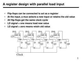
32-bit parallel load register with clock gating Lan Luo • ECE Department, 200 Broun Hall, Auburn University, • Auburn, AL 36849, USA • luolan1@auburn.edu ELEC 6270 Project December 2007
Outline • Concept of Power Dissipation & Clock Gating • Schematics of Basic Cells • Simulation Results • Conclusions • References
Concept of Power Dissipation • Dynamic • Signal transitions (main source) • Logic activity • Glitches • Short-circuit • Static • Leakage
Clock Gating Technique • Clock signal is one of the main sources of chip power: - high switching activity - heavy capacitive loading of the clock network - clock signals in digital computers consume about 15-45% of the system power • Solution: - deactivate the clock signal when there are no transitions on the flip-flops’ input
Clock Gating Circuit Latch free clock gating circuit Latch based clock gating circuit
Design Platform • Latch based clock gating circuit used • Technology: 0.5µm BiCMOS process • EDA Tool: Cadence Spectre (SPICE Simulator) • fCK = 50 MHz • Power measurement • Current from power supply iDD(t) is simulated • Average power Pavg(t) is calculated using integral
1-bit non-clock-gating load register A 2pF/bit load capacitance CL is added to mimic typical clock signal load.
Simulation Results • Case by case comparisons. • Typical case - Input vectors with random transitions • Best case - Input vectors with no transitions • Worst case • Input vectors with transitions in each clock period • Comparisons with different CL for typical case. • CL=0pF, 0.025pF, 0.125pF, 0.25pF, 0.5pF, 1pF, 1.5pF, 2pF, 2.5pF, 3 pF
Typical Case (32-bit) clock-gating non-clock-gating Power reduction: 53.86% !
Case by case comparisons • Typical case (→ typical benefit) • 9.129mW→ 4.212mW, power reduction is 53.86% ! • Best case (→ best benefit) • 9.028mW→ 0.802mW, power reduction is 91.12% ! • Worst case (→ least benefit) • 9.661mW→ 9.345mW, power reduction is 3.27% !
Conclusions • Clock gating technique reduces dynamic power drastically. • The amount of power reduction is input data switching activity dependent. • The larger capacitive loading of clock signal, the more power reduction.
Reference • A. G. M. Strollo and D. De Caro, Low power flip-flop with clock gating on master and slave latches, ELECTRONICS LETTERS, Vol. 36, No. 4, 2000 • Wu, Q., Pedram, M. and Wu, X., Clock-gating and its application to low power design of sequential circuits, CICC, 1997 • Frank Emnett and Mark Biegel, Power Reduction Through RTL Clock Gating, SNUG2000 Thanks !