Download
1 / 28
300 likes | 467 Vues
This senior project presents an in-depth study of Ultra-Wideband (UWB) amplifiers using distributed amplifier design principles. Focused on microstrip line and coplanar waveguide designs, it documents the selection of the NE4210S01 transistor and the derivation of lumped element components based on specific cutoff frequencies. The project details simulations for gain flatness, phase linearity, and stability across various designs. Future work involves de-embedding measurements, optimizing transistor configurations, and fabricating the final circuit layout for testing.

E N D
UWB Amplifier Sarah Kief and Saif Anwar Advisor: Dr. Prasad Shastry 2008 Senior Project Bradley University Electrical Engineering
Outline Where we left off Distributed Amplifier Design Microstrip Line Design Coplanar Wave Guide Design M-derive Design Near future activities
Where we left off Picked transistor - NE4210S01 Cutoff max at 20 GHz Designed lumped element components Design Equations
Where we left off Picked transistor - NE4210S01 Cutoff max at 20 GHz Designed lumped element components Chose biasing parameters from the DC-IV curves Vds=1[V], Vgs=-.45[V]
Bias Point Selection Vds of 2 volts and Ids of 10mA for noise figure.
Where we left off Picked transistor - NE4210S01 Cutoff max at 20 GHz Designed lumped element components Chose biasing parameters from the DC-IV curves Vds=1[V], Vgs=-.45[V] Built / simulated lumped element model with 1 transistor 7 dB
Distributed Amplifier Design Lumped element model built in ADS 2 and 3 transistor designs Simulations Gain flatness Phase linearity Stability
Microstrip Line Design Translated lumped element components into respective lengths and widths in the MSTRIP program Capacitors Zo=30 ohms Inductor Zo=90 ohms Built layout in ADS and simulated Compared microstrip simulation results to lumped element simulations
200 100 0 phase(S(2,1)) -100 m1 freq= 7.085GHz -200 dB(S(2,1))=11.717 3 4 5 6 7 8 9 10 11 Max m1 12 freq, GHz 11 10 9 8 7 dB(S(2,1)) 6 5 4 3 2 1 0 3.0 3.5 4.0 4.5 5.0 5.5 6.0 6.5 7.0 7.5 8.0 8.5 9.0 9.5 10.0 10.5 11.0 freq, GHz Readout Simulations
Coplanar Wave Guide Design Chose RT/Duriod 6002 board Thickness : 20 mils, .508 mm Dielectric Constant : 2.94 1 oz copper plating High mechanical strength
Coplanar Wave Guide Design Design wave guide to test transistors Layout Designed width and length of the layout using Line calc Dimensions Width = 1.017 mm Air Gap = .808 mm Length = 10 mm Constructed layout in ADS Tested and simulated in ADS
M-Derive Design Layout Lm Cm Constant-k LPF M-Derived LPF Need for M-Derived Filter Design • To avoid padding capacitor. • Useful in the layout design. • Easier for optimization purpose.
M-Derive Equations • Lm = L*(k-m2)/4*m • k = m*Cg or Cd / Cm • where Cm = Cin or Cout • Cin=.33 pF, Cout=.1686 pF • Lmd = 1.42 nH (for drain side) • Lmg = 0.004nH (for gate side)
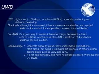
Near future Activities Do De-embedding to find S-Parameters on Coplanar Waveguide Determine the optimal number of transistors Order RT/Duriod Board Test the S-Parameters of the Transistors Optimize the final layout Fabricate and test the circuit