Advance Digital logic Design
360 likes | 380 Vues
Learn about digital and analog electronic circuits, integrated circuits, signal processing, advantages of digital data, ASCII code, and digital-to-analog conversion. Understand the classification and operation of ICs. Explore the importance of digital and analog converters in interfacing with sensors and control systems.

Advance Digital logic Design
E N D
Presentation Transcript
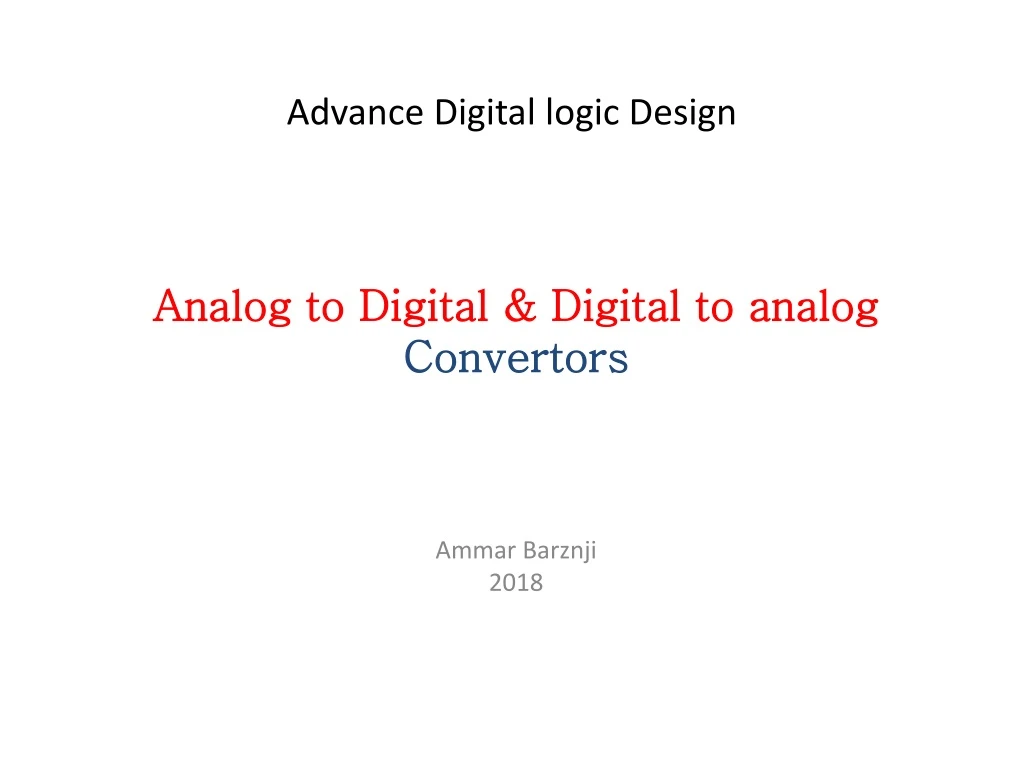
Advance Digital logic Design Analog to Digital & Digital to analog Convertors Ammar Barznji 2018
Electronic circuits can be divided into two broad categories, digital and analog. Therefore there are two types of signals digital signals and analog signals. Digital electronics involves quantities with discrete values, and analog electronics involves quantities with continuous values and can provide infinite number of values according to division size. The Digital Advantages Digital data can be processed, stored and transmitted more efficiently and reliably than analog data.
Digital data has a great advantage when storage is necessary. For example, music when converted to digital form can be stored more compactly and reproduced with greater accuracy and clarity than is possible when it is an analog form. • Noise (unwanted voltage fluctuations) does not affect digital data nearly as much as it does analog signals.
Digital systems are used in communication, business transaction, traffic control, space guidance, medical treatment, weather monitoring, the internet, and many other commercial, industrial, and scientific projects. • We have digital telephones, digital TV’s, digital versatile discs, digital cameras.
Digital Integrated Circuits An integrated circuit (IC) is an electronic circuit that is constructed entirely on a single small chip of silicon. IC packages are classified according to the way they are mounted on printed circuit (PC) boards: The through-hole type packages have pins (leads) that are inserted through holes in the PC board and can be soldered to conductors on the opposite side. (DIP) dual-in-line package. The surface-mount technology (SMT) newer, space-saving, holes are unnecessary. (SOIC) small-outline integrated circuit.
Digital Integrated Circuits Figure 1 ICs
ICs are classified according to their complexity: 1- Small-scale integration (SSI) < 12 gate/chip. They include basic gates and flip-flops Figure 2 SSI ICs
2- Medium-scale integration (MSI) 12 – 99 gate/chip. They include encoders, decoders, counters, registers, multiplexers, small memories. 3- Large-scale integration (LSI) 100 – 9999 gate/chip, including memories. 4- Very large-scale integration (VLSI) 10,000 – 99,999 gate/chip, including (memories and microprocessors). 5- Ultra large-scale integration (ULSI) >100,000. It describes very large memories, larger microprocessors, and large single-chip computers.
ICs are classified according to their operation into Analog IC & Digital IC or both in one. • ICs are classified according to the type of transistors (BJT) bipolar junction transistor and (MOSFET) metal-oxide semiconductor field- effect transistors.
ASCII Code ASCII code (The American Standard Code for Information Interchange) pronounced “askee”. It has 128 characters and symbols represented by a 7-bit binary code. 32 ASCII characters are nongraphic never printed or displayed and used only for control purposes. Others are graphic symbols for printing and displaying.
Digital-Analog Conversion Connecting digital circuitry to sensor devices is simple if the sensor devices are inherently digital themselves. Switches, relays, and encoders are easily interfaced with gate circuits due to the on/off nature of their signals. However, when analog devices are involved, interfacing becomes much more complex. What is needed is a way to electronically translate analog signals into digital (binary) quantities, and vice versa. An analog-to-digital converter, or ADC, performs the former task while a digital-to-analog converter, or DAC, performs the latter.
An ADC inputs an analog electrical signal such as voltage or current and outputs a binary number. In block diagram form, it can be represented as such: A DAC, on the other hand, inputs a binary number and outputs an analog voltage or current signal. In block diagram form, it looks like this:Together, they are often used in digital systems to provide complete interface with analog sensors and output devices for control systems such as those used in automotive engine controls:
It is much easier to convert a digital signal into an analog signal than it is to do the reverse. Therefore, we will begin with DAC circuitry and then move to ADC circuitry. • Digital-to-Analog converters (DACs) and Analog-to-Digital converters (ADC) are important building blocks which interface sensors (e.g. temperature, pressure, light, sound, cruising speed of a car) to digital systems such as microcontrollers or PCs. An ADC takes an analog signal and converts it into a binary one, while a DAC converts a binary signal into an analog value. Figure 3 gives a block diagram of such a system. An example of such a system is a PC sound card.
Figure 3: Digital processing system with an ADC at the input and a DAC at the output Sensor signals vary continuously ("analog") between a specified voltage range. As an example, the output of a microphone gives a voltage between 0 (no speech) to 100mV (for loud speech). Any value between these two extremes are possible. The "analog" signal needs to be converted into a "digital" word of n-bits in order to be read into and processed by a computer (or digital signal processor - DSP). The "analog" and "digital" signals are shown in Figure 3.
Analog-to-Digital Converter An ADC takes an analog input and generates a digital output as shown in Figure 4a. The more bits the output word has the better the resolution. For a 3-bit ADC, the number of steps will be 8 while a 10-bit ADC will divide the analog signal up into 1024 (=210) steps. The input-output relationship of an ADC is shown in Figure 4b for a 3-bit converter. Notice that when the analog input signal (on the horizontal axis) reaches a certain level, a new digital code will be generated (see vertical axis in Figure 4b) which represents the digital output of the ADC as a function of the analog input.
maximum analog signal the ADC can accommodate is called the Full Scale (FS) as is shown in Fig. 4b. As an example, if the analog input is equal to 4/8xFS (Full Scale), the output code for the example of Figure 4b will be (100). However, if one increases the magnitude of the input signal above 4.5/8xFS, the new digital output code will be (101). Figure 4: (a) ADC; (b) input-output characteristics of an Analog-to-Digital Converter
Digital-to-Analog Converter: The input to a DAC is a binary word of n-bits and the output is an analog value, as schematically shown in Figure 5a. Figure 5: (a) DAC block diagram; (b) input-output characteristic of a DAC
The n-bit word (or digital code) is a digital representation of a signal. The relationship between the analog output value and the binary word is for the case of a 3-bit code (b2,b1,bo), as follows: VDAC = K1 (b2/2 + b1 /4 + bo/8) Vref VDAC =(b2/2 + b1 /4 + bo/8) FS in which K1 is a scale factor, Vref is a reference voltage, FS stands for Full Scale (=K1xVref) and bi is the ith bit of the digital word. The bit bo is called the least significant bit (LSB) and b3 is the most significant bit (MSB). Each time the LSB changes the analog output will change by a value equal to FS/23 for a three bit DAC
(or by FS/2N for a N bit DAC). As an example, lets assume that the digital input is equal to (101), K1 = 1 and the reference Vref= 5V. The output voltage will then be: VDAC = K(1/2 + 0/4 +1/8) Vref = 5/8xVref = 5/8xFS = 3.125 V For each digital input (b2,b1,bo) there will be a corresponding output as shown in Figure 5b for a total of 23 = 8 possible digital words. Notice that only discrete values of the output signal are possible. The more bits the input word has, the smaller the steps of the output signal will be (or the better the resolution). Typical ADCs have at least 8 bits of resolution and even 12 to 16 bits are not uncommon. In order to keep the lab manageable we will limit ourselves to building a simple 3-bit DAC and ADC. For more bits, one can extend the same principle by using more components. The scheme used in the lab to build these converetors is only one of many possible designs. For higher resolution converters more sophisticated architectures are used. You will learn more about this in other classes.
1. A practical circuit to implement a DAC converter is a R-2R ladder network, as shown in Figure 6a. Figure 6: (a) R-2R ladder network; (b) Thévenin's equivalent network Do a detailed circuit analysis in your notebook to show that the Thévenin's equivalent resistance and voltage, as shown in Figure 6b, is equal to: RT = R and VT = (V2/2+ V1/4 + Vo/8) You can use the superposition principle to find Thévenin's equivalent voltage.
Why we need data converters? In the real world, most data are available in the form of analog in nature. We have two types of converters analog to digital converter and digital to analog converter. While manipulating the data, these two converting interfaces are essential to digital electronic equipment and an analog electric device which to be processed by a processor in order produce required operation. • For example, take the below DSP illustration, an ADC converts the analog data collected by audio input equipment such as a microphone (sensor), into a digital signal that can be processed by a computer. The computer may add sound effects. Now a DAC will process the digital sound signal back into the analog signal that is used by audio output equipment such as a speaker.
Audio Signal Processing Digital to Analog Converter (DAC) Digital to Analog Converter (DAC) is a device that transforms digital data into an analog signal. According to the Nyquist-Shannon sampling theorem, any sampled data can be reconstructed perfectly with bandwidth and Nyquist criteria. A DAC can reconstruct sampled data into an analog signal with precision. The digital data may be produced from a microprocessor, Application Specific Integrated Circuit (ASIC), or Field Programmable Gate Array (FPGA), but ultimately the data requires the conversion to an analog signal in order to interact with the real world. Basic Digital to Analog Converter D/A Converter Architectures There are two methods commonly used for digital to analog conversion: Weighted Resistors method and the other one is using the R-2R ladder network method. DAC using Weighted Resistors method The below shown schematic diagram is DAC using weighted resistors. The basic operation of DAC is the ability to add inputs that will ultimately correspond to the contributions of the various bits of the digital input. In the voltage domain, that is if the input signals are voltages, the addition of the binary bits can be achieved using the inverting summing amplifier shown in the below figure.
DAC using Weighted Resistors method The below fig 7 shown schematic diagram is DAC using weighted resistors. The basic operation of DAC is the ability to add inputs that will ultimately correspond to the contributions of the various bits of the digital input. In the voltage domain, that is if the input signals are voltages, the addition of the binary bits can be achieved using the inverting summing amplifier shown in the figure above. Applications of Digital to Analog Converter DACs are used in many digital signal processing applications and many more applications. Some of the important applications are discussed below. . Audio Amplifier DACs are used to produce DC voltage gain with Microcontroller commands. Often, the DAC will be incorporated into an entire audio codec which includes signal processing features. . Video Encoder The video encoder system will process a video signal and send digital signals to a variety of DACs to produce analog video signals of various formats, along with optimizing of output levels. As with audio codecs, these ICs may have integrated DACs.
Display Electronics The graphic controller will typically use a lookup table to generate data signals sent to a video DAC for analog outputs such as Red, Green, Blue (RGB) signals to drive a display. Data Acquisition Systems Data to be measured is digitized by an Analog-to-Digital Converter (ADC) and then sent to a processor. The data acquisition will also include a process control end, in which the processor sends feedback data to a DAC for converting to analog signals. Calibration The DAC provides dynamic calibration for gain and voltage offset for accuracy in test and measurement systems. Motor Control Many motor controls require voltage control signals, and a DAC is ideal for this application which may be driven by a processor or controller.
Motor Control Application Data Distribution System Many industrial and factory lines require multiple programmable voltage sources, and this can be generated by a bank of DACs that are multiplexed. The use of a DAC allows the dynamic change of voltages during operation of a system. Digital Potentiometer Almost all digital potentiometers are based on the string DAC architecture. With some reorganization of the resistor/switch array. Software Radio A DAC is used with a Digital Signal Processor (DSP) to convert a signal into analog for transmission in the mixer circuit, and then to the radio’s power amplifier and transmitter.
The image in fig 5 illustrates the use of an ADC, a DAC, and a pair of filters in a digital signal processing (DSP) application. Because processing must be done using digital methods, an ADC is required to convert the analog signals into digital equivalents, and a DAC is needed to convert the processed signals back to analog for compatibility with analog devices. As noted, the filters eliminate harmonic frequencies above the Nyquist frequency and correct other errors inherent in signal conversion.
Zero-Order Hold An immediate difference between digital and analog signals is time. Digital signals are discrete-time signals, meaning they output a sequential series of values, while analog signals are continuous-time with continuous (non-discrete) domains. In order to reconstruct a signal, a typical DAC will latch binary information for a full sample period using a clock signal; this is the reason that digital signals appear as stair-like lines when graphed. Therefore, a low-pass reconstruction filter must be employed to eliminate extraneous harmonics and smooth the signal to render it suitable for output.
Sampling Sampling in digital-to-analog conversion shares similar formulas with analog-to-digital operations. DAC sampling presents some unique challenges, however. A major issue introduced when sampling a digital signal is quantization error (also known as distortion), which results from having multiple inputs (binary bits) for a single output value. Quantization is frequently caused by rounding precise values to the next closest integer, causing distortion of the reconstructed signal. While quantization is a natural occurrence in DAC operation, it can be minimized by using high-resolution devices, since increasing the number of bits increases the gradation scale of the signal. Resolution DAC precision is determined by the number of bits the device possesses. The number of bits, n, is directly related to the number of sampling gradations, N, so that N = 2n. (Gradations can be thought of as the scale of measured intervals which express values contained in the signal to be converted.)
For example, a 12-bit converter is capable of 4096 gradations. If the output signal is within the range of 0-5 V (a typical control signal), this range would be broken up into 4096 intervals in order to match analog or digital values, with 0 V being 0 and 5 V being 4095. If the amplitude of the digital signal is 2000 at a given sample time, the analog output would be 2.4414 V. The entire digital signal can be mapped proportionally using these gradations. Device precision can be defined as 1/N, with smaller values indicating greater precision. For example, a 4-bit converter has a precision 1/16 that of the original signal, while a 10-bit one is 1/1024 as precise. view full size image A sine wave translated using 16-bit (purple) and 4-bit (blue) resolutions. The 16-bit device is capable of 65,528 more gradations than the 3-bit one, resulting in a much more accurate signal. Image credit: National Instruments Design Digital-to-analog converters may use one or several methods (in the case of hybrid devices) for converting a digital signal. Some of the most common are described in the table below.
Fig 8 A sine wave translated using 16-bit (purple) and 3-bit (blue) resolutions. The 16-bit device is capable of 65,528 more gradations than the 3-bit one, resulting in a much more accurate signal.
Sampling A primary stumbling block to analog-to-digital conversion is the difference between analog and digital signals. Analog signals tend to take the form of a continuous wave, while digital ones are purely numerical and, when graphed, take the form of a square wave. Therefore, digital signals may be mapped to analog ones using sampling, the process of measuring the signal at predetermined times. There are two important parameters related to sampling: The sampling rate, fs, determines the number of samples taken per second. Sampling precision, N, determines the gradations for the sampling process. (In other words, sampling precision dictates the y-axis divisions of a graphed signal.)