AsPacker - Bare Die Wirebond Design Tool
AsPacker is a flexible tool for developing Bare Die Wirebond Solutions, aiding engineers in integrating chips into designs efficiently. It ensures design integrity, reliability and ease of use with industry-proven algorithms for superior quality results. The tool simplifies wirebond processes, reduces design time, and offers a user-friendly interface.

AsPacker - Bare Die Wirebond Design Tool
E N D
Presentation Transcript
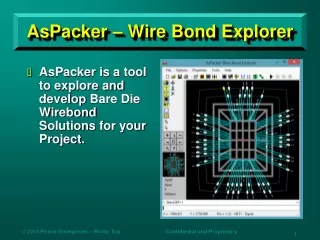
AsPacker – Wire Bond Explorer AsPacker is a tool to explore and develop Bare DieWirebond Solutions for your Project.
AsPacker – Overview • AsPacker aids the engineer integrate bare die or chips into their design. • AsPacker is fully programmable and flexible with many options to explore while trying to achieve the best design possible for your needs. • High pin-out die can be a nightmare to deal with unless you have a tool like AsPacker do the work for you.
AsPacker – Overview • It is simple to use and easy to learn. • Anybody wishing to take advantage of using bare die or chips in their designs will benefit by using AsPacker. • It eliminates the guess work of hand editing by using design rules to drive the process. • For advanced users, AsPaker can be used in the design of Multi Chip Modules, Hybrid Circuits, and Packages.
AsPacker – Overview • By using AsPacker, the time from start to finish is greatly reduced while increasing the design integrity and reliability. • All commands are recorded as they are executed and can be edited and played back at any time. This makes the design process and set-up repeatable, reliable and reusable. • Interface with a PCB/CAD tool is done by using an industry standard LIQ file format.
Industry– Proven Algorithms • The original code stream was developed to assistMCM design houses in the early 1990’s. • The second generation algorithms licensed to Mentor’s PADs and Synopsys’ Sager systems and are still in use today. • The Third generation represents a complete rewrite of the algorithms to allow for a better user interface and integration of multiple tools into a single tool.
Industry– Proven Algorithms • The fourth generation continued to simplify the design process focusing more on the layout engineer eliminating parts of the code that dealt with ASIC design. • The fanout algorithms have been rewritten again toincreasing the accuracy and reliability of the design process through the use of scripting and an easy to understand command language.
Superior QOR (Quality of Results) • Patent Pending algorithm yields superior wirebond results. • Minimum total wirebond length. • Minimum wirebond angles. • Algorithm places die bond pads into geographic groups based on distances between die bond pads and bonds out each group separately. • Other tools center the substrate pads at the geometric center of each side and evenly spread out the pads regardless of gaps between die bond pads. • Can lead to longer wirebonds. • Can create excessive wirebond angles. • AsPacker iteratively looks at multiple solutions and interactions between groups to generate the best final solution. • Total Maximum Iterations can be set (defaults to 100) and the tool will stop before the max iterations if the changes between iterations is less than a set parameter (defaults to .01 micron).
Die with bond pad gaps (typical tool solution) • Notice substrate pads centered creating needless wirebond angles and lengths.
Die with bond pad gaps (AsPacker solution) • Notice AsPacker solution generates minimum wirebond angles and lengths.
Typical Design Flow (1) • Set up work path where design data resides. • Open an LIQ file (short format) or .pinlist file created from the manufacturer’s die datasheet. • Both of these files contain the Die size and thickness along with the CBPs(Component Bond Pad size and location information). • This starts the project and establishes the basic parameters which will be build on. • All the files required for the project should be placed in this project directory. • This also becomes the default directory for other loads, saves, imports and exports.
Typical Design Flow (2a) • Add the number and type of wirebond tiers to be used in the project. • UseTier Properties dialog box to define the tier parameters (Distance from the die, shape and type). • Rings (copper) are generally used for Power and Ground. • Placement guides are used for signals.
Typical Design Flow (2b) • Each tier has it’s own definition and DRC rules. • All units are in microns except for Wire Width which can either be Mils or Microns. • Only those tiers that are used need to be enabled. • Max. Length and Max. Angle are used for post process DRC checks.
Typical Design Flow (3a) • Once the Tiers are defined the Die Attach Pad is added. • Use the Die Attach Pad Tool to define the attach pad. • The attach pad can be tailored to your specific needs. • The inner ring (ground) can optionally be attached to the die.
The Die Attach Pad consists of 3 parts. Die Attach Style, where the die is placed, can be either hatched, solid, or none. Die Attach Margin can be set to the size of the die or over / under sized as needed. Inner Ring Attach Points are the connections to the first tier (ring) from the die attach pad. The back or bottom of the die is electrically called the Back Bias and is usually ground. Typical Design Flow (3b)
Typical Design Flow (4a) • Now you are ready to assign pads to tiers. • Use the Tier Assignment Tool to assign SBPs (Substrate Bond Pads) to the desired tier. • Generally Ground is the inner tier (ring) with Power being the next.
Typical Design Flow (4b) • Assign pads to tiers. • SBPs can be assigned using the Pin name, Package Pin name or Net name. • In the case of signals, you have the option to select multiple pads and split them between specified tiers.
Typical Design Flow (5a) • Generating the Fanout. • Once all the parameters have been set and DRC rules defined in the Tiers Properties dialog box, it is time to generate the SBP fanout. • This is done by using the Fanout Tool.
Typical Design Flow (5b) • Execute Fanout. • There are multiple options that control the fanout process. • You have the option to work on one edge at time or all edges. • You can also select a group of pads and work on only those if desired. • A log is kept as the process runs for review.
Typical Design Flow (6) • The final step is to Export the design. • This is done by using the Export LIQ short format menu option. • Select the features you want to export and click Export. • This produces an LIQ (short format) file that can be imported into a PCB/CAD tool.
Advanced Feature – Stacked Die • Stacked die example. • U2 is placed on U1 by loading the DemoStacked-Die.pinlist • Assign U1 Grounds to tier 1, U1 Powers to tier 2, U1 Signals to tier 3, and U2 all pads to tier 4.
Advanced Feature – Stacked Die • Select all pads on Tiers 1, 2, and 3 using the Select Tool. • Uncheck Keep Pin Order in the Fanout Tool. • Execute fanout on selected tiers.
Advanced Feature – Stacked Die • Unselect tiers 1, 2, and 3 (right mouse click). • Select tier 4 with the Select Tool. • Execute fanout on the selected tier.
Advanced Feature – Stacked Die • The resulting fanout for the Stacked Die is completed and DRC clean. • Wires are allowed to cross because tier 4 is dedicated to U2 signals only and bonded last.
Advanced Feature – Split • Split CBP Example. • CBPs can be split into 2 or more segments to accommodate multiple bond wires (Powers and Grounds). • Use the Split CBP Manager. • Select the CBP to be Split. • Click Split to create segments. • Click Join to rejoin segments.
Advanced Feature – Split • Execute fanout. • One segment in this case is 10 and the other is 10.1. • Select one of the wires (Shift – mouse swipe).
Advanced Feature – Split • Using the Pads Properties dialog box, adjust the CBP wire X and Y offsets. • Do the same for the other CBP segment.
Advanced Feature – Stitch • You can connect CBPs on one die to CBPs on another die by using stitches. • This is a manual process using the Stitch Manager tool.
Advanced Feature – Stitch • You create a Stitch by selecting pads from the 2 drop down lists. • Stitches can be added, edited, or removed. • You can also save and load a stitch list.
Advanced Feature – Script • As mentioned before, all commands are recorded as they are executed and recorded in a time stamped .log. • These logs files can be edited for reuse at a future date as a script .kmd. • This is handy for setting up a project or project parameters. • Scripts are normally have the extension .kmd while the log file extension is .log. • These scripts can be nested to any depth.
Advanced Feature – Script • A script can be executed at the command line by entering “run=“ and script name. • A script can optionally be executed with the toolbar Run option. • Long running scripts or scripts with wait states can be paused with the toolbar Pause option. • Once paused you can step through the script using the toolbar Step option. • To terminate a script, press Escape or the toolbar Stop option.
Options • There are several project options that allow you to visualize the project in different ways as well as how the tool reacts. • Fill CBP Pad enables viewing the CBPs with filled color or just outline. • Display Pad Text displays or hides the CBP and SBP pad text. • Display Die Attach Pad displays or hides the die attach pad and ring connections.
Options • Display All Tool Tips displays of hides the tool tips for controls. • Display Die Only displays only the die if selected. • Die Origin Center if selected the coordinate origin is at the center of the die (default) else it is at the Lower Left Corner of the die. • Reverse Mouse Wheel Zoom Direction reversed how the zoom is done when the mouse wheel is used to zoom in and out. • Cancel Current Operation terminates the current operation and deselects all objects.
Navigation • There are several ways of navigating around the project. • The navigation tool by clicking on one of the 9 buttons to move up, down, right, left, in, out, window view, pan, or view all. • By clicking anywhere in the world view to make that point the center of the view window. • Using the keyboard by holding the CTRL key down while pressing the arrow keys, PgUp, PgDn, and Home to move around the view window.
Selecting Objects • Objects can be selected by either using the Select Tool or by holding down the Shift or CTRL key while clicking on a start point followed by an end point. • Objects within this window are selected. • Once an object is selected you can only select other object of the same type. • To select wires you do the same operation except you swipe across the wires. • A right mouse click or pressing ESC will deselect all objects.
Basic Editing • When objects are selected you have a limited number of editing features. • Move allows you to move selected CBPs or SBPs. • Move to Tier allows you to move selected SBPs to another tier. • Delete will delete selected objects. If a wire is selected the wire and associated SBP are deleted. • These editing features are enabled and disabled based on the objects selected.
Other Tools • The Ruler is used to measure point to point distances by clicking to start and end. As the mouse moves the X and Y deltas and distance are displayed at the bottom of the screen. • The Mouse Wheel is used to zoom in and out. When zooming in the point of the mouse is centered on the screen then zoomed in at that point. • The Middle Mouse Button executes a pan.
Terminology • CBP: Component Bond Pad. • SBP: Substrate Bond Pad. • Wire Bonds: Wires that connect CBPs and SBPs. • Die Attach Pad: The place where the die is placed. • Rings: Copper rings around the Die normally used for Power and Ground. • Stitch: CBP to CBP connections.
Files Included with AsPacker • PDF Files (Help\View\PDF Files …) • CommandSetFormat.pdf list all the commands that can be executed. • LIQFileFormat.pdf explains the various sections that are in the LIQ file. • PinlistFileFormat.pdf explains the various sections that are in the .pinlist file. • ScreenShots.pdf contains images of all the components and tools that make up AsPacker and how to use them. • Split Feature.pdf describes how to use the Split Tool.
Files Included with AsPacker • StitchFeature.pdf explains how to use the Stitch tool. • StitchFileFormat.pdf explains the various sections of the Split file. • Tutorial.pdf walks you through a demonstration project.
Files Included with AsPacker • KMD File (Help\View\KMD Files …) • Demo.kmd executes a basic design from loading a pinlist to generating the fanout. A 1 second wait state has been added after each command. This delay can be eliminated by executing “wait=false” at the command line. • DemoAll.kmd executes the demo.kmd followed by the Split.kmd and the Stitch.kmd. • DieAttachSetup.kmd uses the Attach Tool to set up the Die Attach Pad.
Files Included with AsPacker • Fanout.kmd sets up the fanout parameters and executes the fanout process. • OptionsSetup.kmd sets up all the options used in the Demo.kmd and Demoall.kmd scripts. • Split.kmd demonstrates the use of the Split tool by splitting CBP 11 into 2 segments. • Stitch.kmd demonstrates the Stitch Tool by adding a stacked die on top of the base die and then stitching 2 Power CBPs pads from the stacked die to the base die.
Files Included with AsPacker • TiersAssignmentSetup.kmd assigns all the used CBPs to their proper tiers. • TiersSetup.kmd Sets up the 4 tiers that are used in the Demo and Demoall projects. Tier 1 is a ring for Ground. Tier 2 is a ring for Power. Tier 3 and 4 are placement guides for signals.
Files Included with AsPacker • PinList and LIQ files. • Demo.Pinlist is the input Pin List file used to create the Demo Project. • DemoStackDie.pinlist is the second input file used when the DemoAll.kmd is executed. This demonstrates the use of Stacked Die and Stitching. • DemoShort.liq is an example of the short format LIQ file and can be Imported. • DemoLong.liq is an example of the Long format LIQ file and can be Loaded.