Download
1 / 1
10 likes | 129 Vues
The axial resolution of OCT is equivalent to the coherence length of the light source, which is given by:. where 0 is the central wavelength, and is the linewidth of the spectrum. Congresso del Dipartimento di Fisica Highlights in Physics 2005

E N D
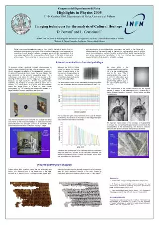
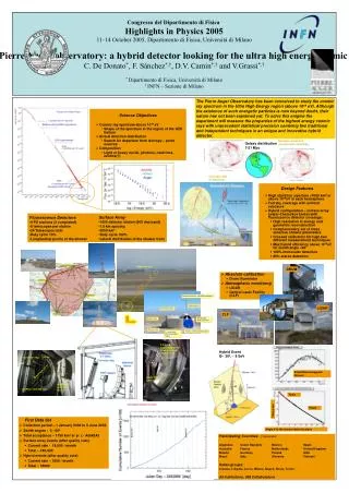
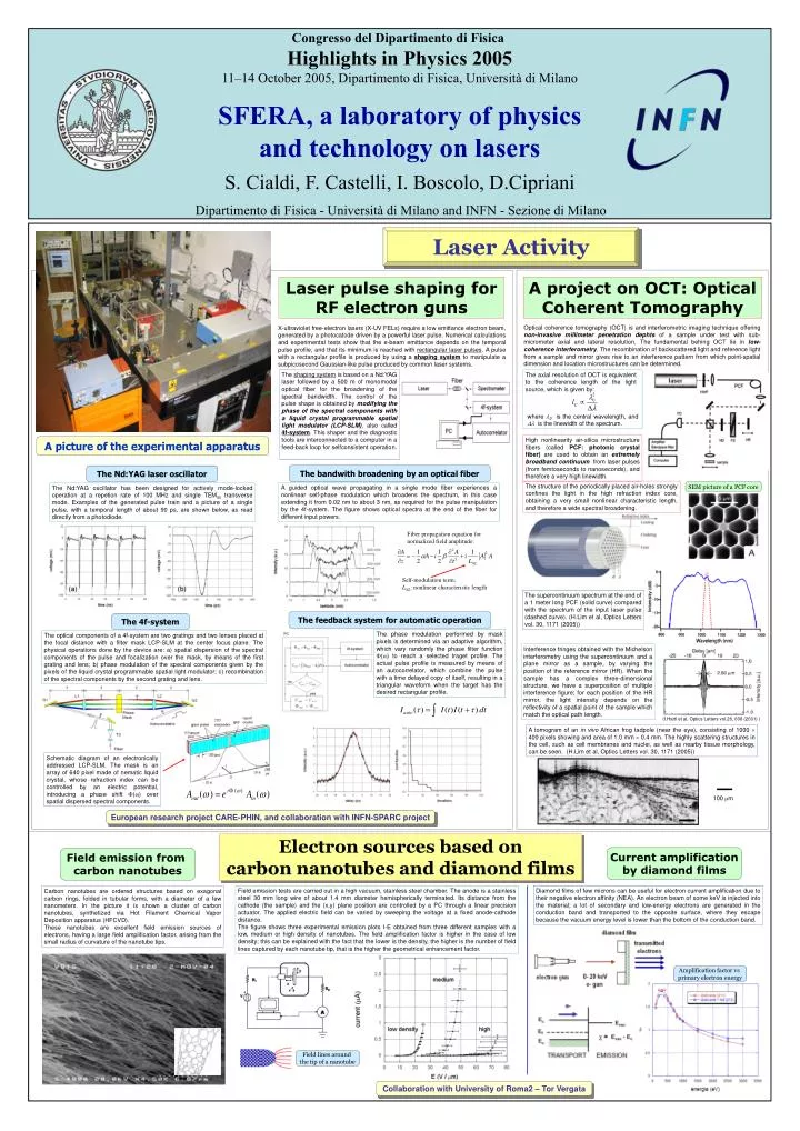
The axial resolution of OCT is equivalent to the coherence length of the light source, which is given by: where 0 is the central wavelength, and is the linewidth of the spectrum. Congresso del Dipartimento di Fisica Highlights in Physics 2005 11–14 October 2005, Dipartimento di Fisica, Università di Milano SFERA, a laboratory of physics and technology on lasers S. Cialdi, F. Castelli, I. Boscolo, D.Cipriani Dipartimento di Fisica - Università di Milano and INFN - Sezione di Milano Laser Activity Laser pulse shaping for RF electron guns A project on OCT: Optical Coherent Tomography Optical coherence tomography (OCT) is and interferometric imaging technique offering non-invasive millimeter penetrationdephts of a sample under test with sub-micrometer axial and lateral resolution. The fundamental behing OCT lie in low-coherence interferometry. The recombination of backscattered light and reference light from a sample and mirror gives rise to an interference pattern from which point-spatial dimension and location microstructures can be determined. X-ultraviolet free-electron lasers (X-UV FELs) require a low emittance electron beam, generated by a photocatode driven by a powerful laser pulse. Numerical calculations and experimental tests show that the e-beam emittance depends on the temporal pulse profile, and that its minimum is reached with rectangular laser pulses. A pulse with a rectangular profile is produced by using a shaping system to manipulate a subpicosecond Gaussian-like pulse produced by common laser systems. The shaping system is based on a Nd:YAG laser followed by a 500 m of monomodal optical fiber for the broadening of the spectral bandwidth. The control of the pulse shape is obtained by modifying the phase of the spectral components with aliquid crystal programmable spatial light modulator (LCP-SLM), also called 4f-system. This shaper and the diagnostic tools are interconnected to a computer in a feed-back loop for selfconsistent operation. High nonlinearity air-silica microstructure fibers (called PCF: photonic crystal fiber) are used to obtain an extremely broadband continuum from laser pulses (from femtoseconds to nanoseconds), and therefore a very high linewidth. A picture of the experimental apparatus The bandwith broadening by an optical fiber The Nd:YAG laser oscillator The structure of the periodically placed air-holes strongly confines the light in the high refraction index core, obtaining a very small nonlinear characteristic length, and therefore a wide spectral broadening. SEM picture of a PCF core A guided optical wave propagating in a single mode fiber experiences a nonlinear self-phase modulation which broadens the spectrum, in this case extending it from 0.02 nm to about 3 nm, as required for the pulse manipulation by the 4f-system. The figure shows optical spectra at the end of the fiber for different input powers. The Nd:YAG oscillator has been designed for actively mode-locked operation at a repetion rate of 100 MHz and single TEM00 transverse mode. Examples of the generated pulse train and a picture of a single pulse, with a temporal length of about 90 ps, are shown below, as read directly from a photodiode. Fiber propagation equation for normalized field amplitude: Self-modulation term; LNL: nonlinear characteristic length The supercontinuum spectrum at the end of a 1 meter long PCF (solid curve) compared with the spectrum of the input laser pulse (dashed curve). (H.Lim et al, Optics Letters vol. 30, 1171 (2005)) The feedback system for automatic operation The 4f-system The phase modulation performed by mask pixels is determined via an adaptive algorithm, which vary randomly the phase filter function () to reach a selected traget profile. The actual pulse profile is measured by means of an autocorrelator, which combine the pulse with a time delayed copy of itself, resulting in a triangular waveform when the target has the desired rectangular profile. The optical components of a 4f-system are two gratings and two lenses placed at the focal distance with a filter mask LCP-SLM at the center focus plane. The physical operations done by the device are: a) spatial dispersion of the spectral components of the pulse and focalization over the mask, by means of the first grating and lens; b) phase modulation of the spectral components given by the pixels of the liquid crystal programmable spatial light modulator; c) recombination of the spectral components by the second grating and lens. Interference fringes obtained with the Michelson interferometry using the supercontinuum and a plane mirror as a sample, by varying the position of the reference mirror (HR). When the sample has a complex three-dimensional structure, we have a superposition of multiple interference figure; for each position of the HR mirror, the light intensity depends on the reflectivity of a spatial point of the sample which match the optical path length. (I.Hartl et al, Optics Letters vol.26, 608 (2001) ) A tomogram of an in vivo African frog tadpole (near the eye), consisting of 1000 400 pixels showing and area of 1.0 mm 0.4 mm. The highly scattering structures in the cell, such as cell membranes and nuclei, as well as nearby tissue morphology, can be seen. (H.Lim et al, Optics Letters vol. 30, 1171 (2005)) Schematic diagram of an electronically addressed LCP-SLM. The mask is an array of 640 pixel made of nematic liquid crystal, whose refraction index can be controlled by an electric potential, introducing a phase shift () over spatial dispersed spectral components. 100 m European research project CARE-PHIN, and collaboration with INFN-SPARC project Electron sources based on carbon nanotubes and diamond films Current amplification by diamond films Field emission from carbon nanotubes Field emission tests are carried out in a high vacuum, stainless steel chamber. The anode is a stainless steel 30 mm long wire of about 1.4 mm diameter hemispherically terminated. Its distance from the cathode (the sample) and the (x,y) plane position are controlled by a PC through a linear precision actuator. The applied electric field can be varied by sweeping the voltage at a fixed anode-cathode distance. The figure shows three experimental emission plots I-E obtained from three different samples with a low, medium or high density of nanotubes. The field amplification factor is higher in the case of low density; this can be explained with the fact that the lower is the density, the higher is the number of field lines captured by each nanotube tip, that is the higher the geometrical enhancement factor. Diamond films of few microns can be useful for electron current amplification due to their negative electron affinity (NEA). An electron beam of some keV is injected into the material; a lot of secondary and low-energy electrons are generated in the conduction band and transported to the opposite surface, where they escape because the vacuum energy level is lower than the bottom of the conduction band. Carbon nanotubes are ordered structures based on exagonal carbon rings, folded in tubular forms, with a diameter of a few nanometers. In the picture it is shown a cluster of carbon nanotubes, synthetized via Hot Filament Chemical Vapor Deposition apparatus (HFCVD). These nanotubes are excellent field emission sources of electrons, having a large field amplification factor, arising from the small radius of curvature of the nanotube tips. Amplification factor vs primary electron energy Field lines around the tip of a nanotube Collaboration with University of Roma2 – Tor Vergata