Carbon Nanotube Research
70 likes | 325 Vues
Carbon Nanotube Research. Robert A. Sayer July 16, 2010 School of Mechanical Engineering, and Birck Nanotechnology Center Purdue University. What is a Carbon Nanotube (CNT). Formed from the hexagonal graphene carbon structure Can take single-wall (SWCNT) or multi-wall (MWCNT) structures

Carbon Nanotube Research
E N D
Presentation Transcript
Carbon Nanotube Research Robert A. Sayer July 16, 2010 School of Mechanical Engineering, and Birck Nanotechnology Center Purdue University
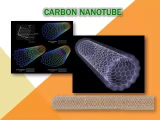
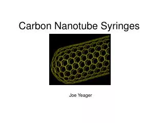
What is a Carbon Nanotube (CNT) • Formed from the hexagonal graphene carbon structure • Can take single-wall (SWCNT) or multi-wall (MWCNT) structures • Ends (tips) can be open or closed (capped) • Excellent material properties M. Terrones, Annu. Rev. Mater. Res. 33 (2003)
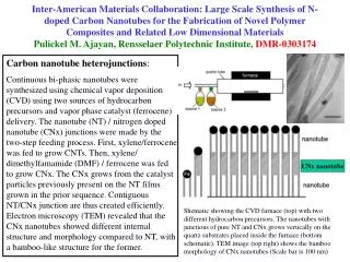
Growing CNTs: Microwave Plasma Chemical Vapor Deposition Process gases: H2 – 50cm3/min CH4 - 10cm3/min 1.5kW@2.5GHz Microwave Generator Vacuum Chamber Substrate Bias: 0 – 600 V; 0 – 1.7 A Dual Wavelength Pyrometer Stage Temperature Control with Heating up to 1000oC 75 mm of Stage Translation External Interlocks for Safe Operation Seki Technotron Corp. AX5200 Series
CNT Electronics: Vertical Devices Fabrication based work Processes include: metal evaporation, e-beam lithography, anodization, CNT growth, electrodeposition, RIE etching, sputtering SWCNTs grown in vertically using a porous anodic alumina (PAA) template Vertical devices have a much smaller footprint than planar devices Current devices are planar Do not take advantage of the aspect ratio of CNTs Vertical devices have a packing density of 100/μm2 200 nm
Self-Heating of CNT Devices: Noise Thermometry • Due to the small size of CNTs, very high current densities (~ 108 A/cm2) arise in biased devices • Temperature rise on the order of hundreds of Kelvin observed • Electrical noise thermometry used to measure the heating of devices during operation • Relates the magnitude of electrical noise inherent in the system to temperature • Thermal resistance: R =1.5 x 10⁸ ± 0.1 x 10⁸ K/W • Compares well with recent estimate of interface resistance between a metallic SWCNT and a dielectric substrate (5.8 Km/W)[Pop et al.J. Appl. Phys. 101 093710 (2007)] Figure: Normalized current spectrum of a SWCNT array
