Carbon Nanotube Quantum Resistor
400 likes | 698 Vues
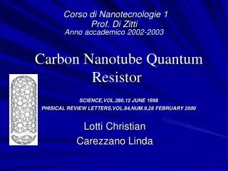
Corso di Nanotecnologie 1 Prof. Di Zitti Anno accademico 2002-2003. Carbon Nanotube Quantum Resistor. Lotti Christian Carezzano Linda. SCIENCE,VOL.280,12 JUNE 1998 PHISICAL REVIEW LETTERS,VOL.84,NUM.9,28 FEBRUARY 2000. Carbon Nanotube. History and Definition:

Carbon Nanotube Quantum Resistor
E N D
Presentation Transcript
Corso di Nanotecnologie 1 Prof. Di Zitti Anno accademico 2002-2003 Carbon Nanotube Quantum Resistor Lotti Christian Carezzano Linda SCIENCE,VOL.280,12 JUNE 1998 PHISICAL REVIEW LETTERS,VOL.84,NUM.9,28 FEBRUARY 2000
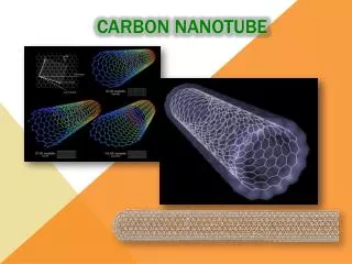
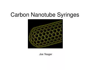
Carbon Nanotube • History and Definition: • Nanotube were discovered in 1991 by Sumio Iijima who produced them by vaporizing carbon graphite with an electric arc under an inert atmosphere. • Nanotubes are long, cylindrical carbon structures consisting of hexagonal graphite molecules attached at the edges.
Carbon Nanotube • Multiwall Nanotube (MWNT) 1991: consist of several nested cylinders with an interlayer spacing of 0.34 – 0.36 nm that is close to the typical spacing of turbostratic graphite.
Carbon Nanotube • Multi-wall Nanotubes by Tunneling Electron Microscope
Carbon Nanotube • Singlewall Nanotube (SWNT) 1993: in the ideal case, a carbon nanotube consist of either one cylindrical graphene sheet.
Carbon Nanotube • Carbon nanotubes are now considered to be the building blocks of future nanoscale electronic and mechanical devices. Hence the importance of studing their conducting behaviour.
Quantized Conductance • Fundamental hypothesis: Considering MWNT as an extremely fine and constricted wave guide with a length smaller than the electronic mean free path. Electronic transport is ballistic: every electron injected into the nanotube at one end come out the other end.
Quantized Conductance • Ballistic Transport involved: • G0contribute to conductance of every conducting channel. • No energy dissipation along the nanotube conductor.
Quantized Conductance • G0 is the fundamental quantum of conductance: • e is the charge on the electron • h is the Planck constant
Multiwall Nanotube Conductance • In order to verify the quantized conducting behaviour of nanotubes in 1998 Walt de Heer invented an ingenious way to measure the electrical conductance of MWNTs.
Experimental Scheme • Using arc discharge process were produced very fine and compact fibers composed of carbon nanotubes and graphitic particles. Schematics of an arc discharge
Experimental Scheme • The nanotube fiber was attached to a gold wire with colloidal silver paint. • The fiber is a bundled of nanotubes with different lenghts and it has been seen that one MWNT protruding from the tip of the fiber. Carbon fiber TEM micrograpy
Experimental Scheme • nanotubes` length 1-10 µm • nanotubes` diameter 5-25 nm Transmission electron micrograph of the end of a nanotube fibe recovered from a nanotube arc deposit
Experimental Scheme • nanotubes` inner cavities 1-4 nm • nanotubes` layers up to 15
Experimental Scheme • The nanotube contact was installed in place of the tip of a scanning probe microscope. Below the nanotube contact there was a heatable copper reservoir containing mercury.
Experimental Scheme • A macroscopic fiber of multiwall nanotubes was lowered into a drop of liquid metal. Because individual nanotubes stick out from the fiber, by dipping the nanotubes to different depths is possible to determine the resistance of individual nanotubes. Vappotential (10-50 mV) was applied to the contact, the current through the circuit was measured together with the piezo displacement.
Results • This figure shows conductance versus time; the nanotube contact is moved at constant speed into and out of the liquid metal.
Results • The period of motion is 2 s, the conductance jumps to ~ 1G0 and then remains constant for ~ 2 µm of its dipping depth. Nanotube is a quantized conductor
Results • This figurepresents a sequence of steps at 1G0 intervals, because other tubes come into contact with the liquid metal. After a dipping distance of 200 nm there is a second step (the second tube comes into contact with the metal ~200nm after the first).
Results • The conductance does not immediately rise to G0 but is ~ 0,5 G0 for the first 25nm This effect can be related to the tip structure of the nanotubes.
Results • The ~ 30% of the nanotubes have tapered tips • The conductance was reduced due to the presence of the tip-to-shaft interface
Results • This plot (G0 versus z-position) is the tip effect; the scanning range was reduced to 70 nm.
Results • The figure B is the histogram of the conductance data of all 250 traces in the sequence represented in Fig. A. • The plateus at 1G0 and at 0 produce peaks in the histogram.
Results • Histogram of a nanotube with several liquid metal (mercury,cerrolow,gallium). The type of liquid metal used in LMC does not effect the properties reported above
Conclusion • The nanotubes were not dameged even at high voltages (Vap=6V J>107Acm-2) for extended times. Power dissipated = 3 mW Bulk thermal conductivity = 10 Wcm-1K-1 We would attain a temperature Tmax=20000°K Impossible: nanotubes start to burn at~700°C
Conclusion • Heat is dissipated in the leads to the ballistic element and not in the element itself.
Conclusion • The conductance of MWNTs has been observed to be G~1G0 and it’s independent of the number of layers because by geometrical and energetical evidence only one layer can conduct.
Unsolved problem • As shown the conductance of nanotubes seems to have a behaviour in disagreement with theoretical prediction: the conductance in MWNTs was observed to be 1G0 instead of 2G0.
MTWNs’ Fractional Quantum Conductance • Using a scattering tecnique based on a parametrized linear combination of atomic orbitals Hamiltonian, Sanvito, Kwon, Tomanek and Lambert calculate the conductance and find the reason of the phenomena observed in Walt de Heer’s experiment.
MTWNs’ Fractional Quantum Conductance • The work is based on the consideration that MWNTs have a finite lenght and a non-homogeneous structure. • This leads to strong interwall interactions that blocked some of the conduction channels and are responsible of a non-uniform redistribution of the total current density over the individual tube walls.
MTWNs’ Fractional Quantum Conductance • The key problem in explaining de Heer’s experimental data was that nothing was known about the MWNTs’ internal structure and about the nature of the contact between nanotubes and Au and Hg electrodes. Tomanek and his group start their calculation assuming the following scenario.
MTWNs’ Fractional Quantum Conductance • Hypotesis: • Current injection from the gold electrode occurs only into the outermost tube wall. • Chemical potential equals that of mercury, shifted by a contact potential, only within the submersed portion of the tube.
MTWNs’ Fractional Quantum Conductance • This is the scheme of the inhomogenous structure of the MWNT. It’s to note that even if only the outer layer is in direct contact with Hg electrode, we can consider equipotential with mercury all the layers immersed into Hg. • Hg(#1) – single-wall MWNT’s portion eq. with Hg. Hg(#2) – double-wall MWNT’s portion eq with Hg. Hg(#3) – triple-wall MWNT’s portion eq with Hg.
MTWNs’ Fractional Quantum Conductance • (b) the calculation for submersion depth Hg(#1) consider a scattering region consisting in a finite length triple-wall nanotube connected to another finite double-wall nanotube region; this is then connected to an external semi-infinite single-wall SWNT.
MTWNs’ Fractional Quantum Conductance • (c) calculation for depth Hg(#2) consider a scattering region made up of a finite-length triple-wall nanotube segment attached a SWNT on one end and to a double-wall nanotube on the other one.
MTWNs’ Fractional Quantum Conductance • (d) calculation for depth Hg(#3) consider a triple-wall nanotube in contact with a SWNT lead.
MTWNs’ Fractional Quantum Conductance • The calculated conductance depend also on the Fermi level that lies within the narrow energy window indicated by the grey region in the previous pictures.
MTWNs’ Fractional Quantum Conductance • The results of the calculation show that also in theoretical predictions conductance increase in discrete step of 0.5G0 until the value of 1G0.G does not exceed this value because only the single-wall portion of the MWNT is in direct contact with the gold electrode.
MTWNs’ Fractional Quantum Conductance • In summary it has been shown that fractional quantum conductance may occur in multiwall nanotubes due to interwall interaction that modify the density of state near the Fermi level, and due to tube inhomogeneities, such as a varying number of walls along the tube.
