Download
1 / 19
240 likes | 777 Vues
Electronic Structure of Single-Walled Carbon Nanotubes (SWNT) . Nan Zheng Solid State II Instructor: Elbio Dagotto Spring 2008 Department of Physics University of Tennessee Email: nzheng@utk.edu.

E N D
Electronic Structure of Single-Walled Carbon Nanotubes (SWNT) Nan Zheng Solid State II Instructor: Elbio Dagotto Spring 2008 Department of Physics University of Tennessee Email: nzheng@utk.edu
Outline • Introduction • Band Structure Calculation • Conducting Properties and Applications • Summary
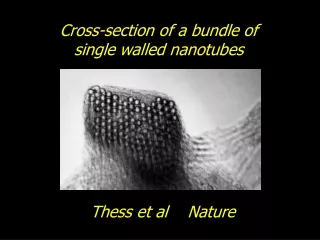
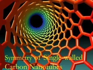
Introduction I: structures overview A: armchair SWNT B: zigzag SWNT C: chiral SWNT D: helical structure of SWNT(TEM) E: a MWNT (TEM) F: a packing of lots of SWNTs (TEM) G: nanotube forest of MWNTs (SEM)
Introduction III: defining strucures Chiral vector (m,n) describes how to “roll up” the graphene sheet to make nanotubes. Three types of SWNTs: 1. Zigzag (m=0 or n=0) 2. Armchair (m=n) 3. Chiral (others)
Introduction IV: Semiconductor or metal? Experimental Facts: • Graphene Semi-Metal • Single-Walled Carbon Nanotubes • All armchair SWNTs (m=n) are metals • Those with n-m=3I (I is a non-zero integer) are semiconductors with tiny (~meV) band gap (or semimetals) • Others are semiconductors with band gap dependent on nanotube diameter
Band Structure Calculation I: introduction to tight binding approach • Idea:construct linear combination of atomic wavefunctions of each unit cell to achieve blochwavefunction. • Secular Equation: with where H is transfer integral matrix; S is overlap integral matrix; C is a vector with all coefficients of bloch wave in terms of atomic wavefunctions.
Band Structure Calculation I: introduction to tight binding approach • How: • Specify unit cell and unit vectors; • Specify Brillouin zone and reciprocal lattice vectors. Select high symmetry directions and momentum along the high symmetry axes; • For the selected momentum points, calculate the transfer and overlap matrix element, H and S. • For the selected momentum points, solve the secular equation and obtain the eigenvalues and eigenstates.
Band Structure Calculation II: Graphene First Graphene lattice Reciprocal lattice Nearest Neighbor Assumption: ( is called transferred integral constant) Linear combination of the three nearest neighbors:
Band Structure Calculation II: Graphene First • Transfer and overlapping matrices: • Solving secular equation gives:
Band Structure Calculation III: Carbon Nanotube • How : Adding periodic boundary conditionto graphene tight- binding calculation along the circumferential direction. • Example : For armchair structure (m=n), (with n to be the chiral integer) Dispersion relation
Band Structure Calculation III: Carbon Nanotube • General result for carbon nanotube: • Nanotubes with n-m=3I, where I is a integer, are metals with no energy gap; • Others are semiconductors with a bandgap which decreases with the increase in nanotube diameter: with
Band Structure Calculation III: Carbon Nanotube • Comparing with Experiment: • All armchair nanotubes (m=n) are metallic • Nanotubes satisfying m-n=3I develops a tiny band gap (for example, a 10A nanotube has a 40meV gap) • Nanotubesnot satisfying m-n=3I are semiconductors with an energy gap inversely varied with diameter (for example, a 10A nanotube has a 1eV gap) • Deviation from experiment due to curvature: • The transitional integral constants ( s) of the three nearest neighbors are not identical • Hybridization becomes important
Conducting Properties and Applications I: Conducting Properties • Metallic CNTshave remarkable conducting ability: Electrons can travel as long as several micrometers without being back scattered. (compare with copper: scattering length being several nanometers) • Conductance of semiconducting CNTs are as good as copper when gate voltage increases • Reason: Electrons in 1D system can only be scattered by completely reversing its direction, while in higher dimensional systems scattering can occur even by a small angle.
Conducting Properties and Application II: Semiconducting CNTs as transistors • Advantages of semiconducting CNTs: • Small size (of course!) • No more surface states in 3D materials
Conducting Properties and Application III: Novel Device: Rectifier
Summary • Carbon nanotubescan be semiconductor or metallic depending on their chiral structures. Main physics can be achieved using nearest neighbor tight binding approach. • Remarkable electronic properties of both metallic and semiconducting carbon nanotubes make them promising candidate material for future molecular devices. • Challenges for eventual application: • Fabrication in a controlled fashion • Integration into existing microelectronic system
References [1] S. G. Louie, Top. Appl. Phys. 80, 113 (2001). [2] J. W. G. Wildoer, L. C. Venema, A. G. Rinzler, R. E. Smalley, C. Dekker, Nature 391, 59 (1998). [3] A. Thess et al., Science 273, 483 (1996). [4] R. H. Baughman et al., Science 297, 787 (2002). [5] M. P. Anantram and F. Leonard, Rep. Pro. Phys. 69, 507 (2006). [6] G. S. Painter and D. E. Ellis, Phys. Rev. B 1, 4747 (1970) [7] R. Saito, G. Dresselhaus and M.. S. Dresselhaus, Physical Properties of Carbon Nanotubes, Imperial College Press (1998) [8] R. A. Jishi, et al., J. Phys. Soc. Jpn. 63, 2252 (1994) [9] C. T. White, D. H. Robertson and J. W. Mintmire, Phys. Rev. B 47, 5485 (1993). [10] C. T. White and J. W. Mintmire, J. Phys. Chem. B 109, 52 (2005). [11] J. W. Mintmire and C. T. White, Phys. Rev. Lett. 81, 2506 (1998). [12] I. Cabria, J. W. Mintmire and C. T. White, Phys. Rev. B 67, 121406 (2003). [13] X. Blase et al., Phys. Rev. Lett. 72, 1878 (1994). [14] P. L. McEuen, Physics World 13, 31 (2000). [15] L. Kouwenhoven and C. Marcus, Physics World 11, 35 (1998). [16] W. H. A de, R. Martel, Physics World 13, 49 (2000). [17] http://en.wikipedia.org/wiki/Carbon_nanotube