Download
1 / 17
170 likes | 356 Vues
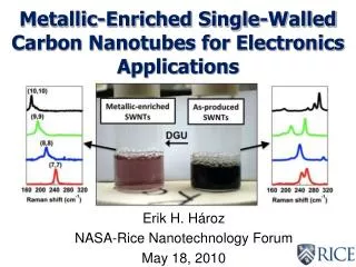
Metallic-Enriched Single-Walled Carbon Nanotubes for Electronics Applications. Erik H. Hároz NASA-Rice Nanotechnology Forum May 18, 2010. a 2. Single-Walled Carbon Nanotubes. a 1. ( n , m ) = (4,2). Chiral vector:. C h = n a 1 + m a 2. n – m = 3 M + q. 1) M = q = 0.

E N D
Metallic-Enriched Single-Walled Carbon Nanotubes for Electronics Applications Erik H. Hároz NASA-Rice Nanotechnology Forum May 18, 2010
a2 Single-Walled Carbon Nanotubes a1 (n,m) = (4,2) Chiral vector: Ch = na1 + ma2 n – m = 3M + q 1) M = q = 0 Metal (Armchair) 2) M≠0,q = 0 Narrow Gap Semicond. 3) M≠0,q = ±1 Metallic Semiconducting Wide Gap Semicond.
“Metallic” Carbon Nanotubes • Metallic SWNTs can be divided into two subclasses, identifiable by their chiral indices (n,m): • True metallic or “armchair” nanotubes where (n-m)=0 such as the (7,7) • Narrow-gap semiconducting nanotubes where (n-m) = integer multiple of 3 such as the (12,6) • Are ballistic conductors with electrical conductivity 100x greater than copper and electron mobility 70x that of silicon. Current-carrying capacity 109 A/cm2. • Ideal materials for low-loss, high-capacity, power transmission cables and nanometer-sized electronics. Tans et al., Nature, 386, (1997), 474 • Problems studying metallic SWNTs: • In bulk material, theoretically, 1/3 of all possible chiralities are “metallics”. Outnumbered by semiconductors. • In HiPco SWNTs, E22 semiconducting transitions overlap with E11 metallic transitions. • Radial breathing mode of armchair SWNTs is very weak in Raman spectra as compared to other chiralities because the electron-phonon coupling being weakest for armchair SWNTs. Solution: Make samples consisting of all “metallic” SWNTs.
Density Gradient Ultracentrifugation Metallic-enriched SWNTs As-produced SWNTs DGU HiPco HPR 188.1 SWNTs suspended in 1% sodium deoxycholate (1mg/mL starting conc.) Sonicated for about 30 min in bath sonicator, 20 hr in tip sonicator, Decant prepared using 1hr centrifugation @ 200,000g Run in a 40-20% iodixanol gradient in 1.5% sodium dodecyl sulfate, 1.5% sodium cholate Centrifugated for 18 hrs @ 200,000g • Arnold et al., Nature Nanotechnology, 1, (2006), 60 • -Optical Absoprtion Characterization and sheet conductance measurements • Yanagi et al., Applied Physics Express, 1, (2008), 034003 • -Optical Absorption & Single-line Excitation Raman characterization • Iijima, et al., Nano Letters, 8, (2008), 3151 • - E-beam diffraction TEM chirality assignment of Kataura sample
Absorption Spectroscopy • Peaks correspond to absorption of light at energies corresponding to excitonic transitions of specific (n,m) species of SWNTs • Transitions are roughly proportional to inverse diameter but also depend on chiral angle and mod # as well. • Absorption is most direct optical method to measure (n,m) species populations. • Sharpness of features and slope of baseline qualitatively indicate degree of individuality. • Sharp, narrow, well-defined peaks with large absorbance in E11M region. • Flat, featureless section in E22S & E11S regions. • Overlap between E11M & E22S regions eliminated. • Absorption features have enhanced peak-to-valley ratios. • Decrease in baseline of spectrum indicates increase in degree of individuality. • Based on absorption peak areas, sample is 98% metallic. x 0.1 x 2
Photoluminescence Excitation Spectroscopy Starting SWNT material Metallic-enriched SWNTs • Only individualized, wide-gap semiconducting SWNTs fluoresce in the • near-infrared via visible excitation. • Individualized, narrow-gap semiconducting SWNTs, armchair SWNTs, • and bundles of SWNTs containing metallics do not fluoresce.
Resonant Raman Spectroscopy • Resonant Raman scattering with a tunable excitation source is the only optical method able to identify all chiralities present, including the armchairs (n,n). • Using excitation sources including: • CW Ti:Sapphire laser (695-850 nm) • Kiton red laser dye (610-685 nm), • Rhodamine 6G+B laser dye (562-615 nm), • Ar+ laser (514.5, 501.7, 496.5, 488, 476.5, & 457.8 nm) • doubled CW Ti:Sapphire (500-440 nm) • 5 weeks and 230 spectra later….
Raman (562-670 nm) Metallic-enriched HiPco As-produced HiPco
Raman (440-500 nm) Metallic-enriched HiPco As-produced HiPco
Enrichment of Armchair Nanotubes • Probing further using Raman scattering, we find not only did we enrich in metallic nanotubes but… • Of those metallic species, a large majority (~50%) are armchairs (n,n). Results summarized in Hároz et al., ACS Nano4, 1955 (2010).
Absorption of Films: UV-vis-NIR • 100% SWNT films produced by vacuum filtration from DGU-enriched solutions. • Sharp, narrow, well-defined peaks with large absorbance in E11M region. • Metallic features remain relatively unperturbed in film form probably due to screening. • Broadened, redshifted peaks in E22S & E11S regions.
RBM Raman of DGU Films (7,7) 514 nm excitation Very little iodixanol • Enrichment results in suppression of (8,5), (9,3) & (8,2) leaves behind mostly (7,7). • Very little density gradient medium left. (8,5) (8,2) (9,3)
Absorption of Films: Terahertz • THz examines optical conductivity. • Response thought to be due to concentration of metallic SWNTs (i.e. THz absorbance proportional to conductivity). • Although metallic films have lower overall optical absorption, they possess greater more metallic nanotubes.
How can these materials be used in research? • In the Kono group, we are using these enriched materials to look at • Temp. dependent DC magneto-transport • Optical spectroscopy • Electron spin resonance • Ultrafast spectroscopy • Terahertz conductivity • Pump-probe • We are also looking at ways to scale separations using column chromatography
Armchair Quantum Wire Program • More broadly at Rice, we are engaged in trying to create macroscopic structures (films and wires) comprised of armchair nanotubes. • Primary question to answer: • While individual armchair SWNTs are excellent ballistic conductors, how about in macrostructures? • What dominates, tunneling barriers (i.e. variable range hopping)? Can this be overcome?
Acknowledgements • Prof. JunichiroKono (Rice, advisor) • Prof. R. Bruce Weisman (Rice) • Dr. Stephen K. Doorn (LANL) • Dr. Robert H. Hauge (Rice) • Mr. William D. Rice (Rice) • Mr. SaunabGhosh (Rice) • Mr. Benjamin Y. Lu (Rice) • Mr. Budihpta Dan (Rice) • Mr. Lei Ren (Rice) • Funding provided by DOE, AFRL, NSF, LANL LDRD program, and Welch Foundation.