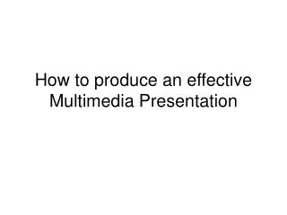
HOW TO PRODUCE PCB
HOW TO PRODUCE PCB . Instructions of making PCB by using Negative Film Resist By: FYP @ PCB Fabrication Lab Telecommunication Engineering Department. FKEKK, UTeM. STEP 1 : PRINT THE ARTWORK.

HOW TO PRODUCE PCB
E N D
Presentation Transcript
HOW TO PRODUCE PCB Instructions of making PCB by using Negative Film Resist By: FYP @ PCB Fabrication Lab Telecommunication Engineering Department. FKEKK, UTeM
STEP 1 : PRINT THE ARTWORK • FINALIZE THE CIRCUIT TO BE PRINTOUT. PRINT ONLY THE TOP @BOTTOM LAYER WITHOUT TOP@BOTTOM SILK MASK • NAME SHOULD BE MIRRORED • PRINT THE ARTWORK ON THE TRASPERANCY SHEET • THE ARTWORT SHOULD BE PRINT IN THE NEGATIVE IMAGE (WHITE CIRCUIT WITH BLACK BACKGROUND) • IT IS IMPORTANT TO PRINT IN HIGH RESOLUTION OTHERWISE PRINT THE ARTWORK IN TWO COPIES AND COMPLIES TOGETHER TO GET THE BLACK AREA IN HIGH BLACK RESOLUTION. • PRINTING MAY BE FROM LASERJET OR BUBBLE JET. BUT THE BEST IS BY USING A LASER JET PRINTER.
STEP 2 : CLEAN THE BOARD • Choose the copper board and clean with very fine grade of sand paper. For best results, clean the board using fine steel wool or similar abrasive pad. After cleans rinse the copper board with water. This will remove dirt, oils, and other contaminationon the top of the copper board. • The board must be absolutely clean and dry prior to applying film. (Note: After rinse, the board should be dried quickly to avoid oxidization.)
Copper board before cleaning with fine steel wool/sand paper
Step 2: CUT THE DRY FILM FOTORESIST Work in a safe light environment when handling the film – any exposure to UV light will expose the film. Safe light refers to any incandescent bulb less than 40 watts.
Step 2: CUT THE DRY FILM FOTORESIST • Sharp scissors @ knife work best for cutting this film. The amount of film required depends on the size of the board being laminated. A 1 cm border should be left on all sides of the board due to shrinkage from heat. (See diagram 2b)
Step 2: CUT THE DRY FILM FOTORESIST • For double sided boards, cut the film big enough (one piece) to sandwich the board in the middle. (See diagram 3c) For a double-sided board, you will only have the 1 cm border on 3 sides. No border is required for the side where the film meets the board.
STEP 3 : REMOVE THE PROTECTIVE LAYER AND APPLY THE FILM • First peel off the protective coating (on the side with the sticker - the soft hazzy side).Apply the film face down with the side that just had the film removed. Fold back the film on the side that will be fed into the laminator. (See diagram 3b) It is important that the film is wrinkle free.For a double-sided board, no folding is required as the board is already sandwiched between the film. (See diagram 3c)
STEP 4 : LAMINATE THE DRY FILM FOTORESIST • Turn on the laminator. Set the temp to 120C. Wait until the laminator ‘ready’ indicator is on. Feed the board with the film side facing up into the laminator. Feed the side of the board with the excess border folded back. • Once the board finishes laminating, put it through the laminator for a second time immediately after the first run (if required). The process is the same for the double-sided board.
LAMINATING THE DRY FILM FOTORESIST ON THE TOP OF THE COPPER SURFACE
LAMINATED DRY FILM RESISIT ON THE COPPER BOARD TOP PROTECTIVE LAYER DRY FILM RESIST COPPER LAYER
STEP 5 : EXPOSING THE BOARD • EXPOSING THE DRY FILM RESIST PROCESS IS TO TRANSFER THE ARTWORK CIRCUIT AT THE TOP OF THE BOARD. • THIS PROCESS REQUIRES UV LIGHT WITH 375nm WAVELENGTH @ UV EXPOSING UNIT • THE PRINTOUT WILL BE ACT AS A MASK. • THE RESIST AREA WHICH THE UV LIGHT GO THRU WILL BECAME DARKER AND VICE VERSE. • POSITION THE ARTWORK IN CONTACT WITH THE RESIST SIDE OF THE COPPER BOARD AND PLACE DOWN BOTH IN THE UV EXPOSURE UNIT. • HAVING CLOSE THE LID , SET THE TIME TO 30 SEC OF THE EXPOSING TIME FOR THE DRY FILM. • THE ARTWORK CAN BE SEEN LIGHTLY AT THE TOP OF THE BOARD AFTER EXPOSING PROCESS.
IMPORTANT TO CONCERN! • PIN 1 OF THE IC (INTEGRATED CIRCUIT) AT THE RIGHT TOP SIDE • WIPE THE TOP GLASS WITH DRY CLOTH TO MAKE SURE THEY ARE CLEAN FROM DUST. • CLOSE THE UV EXPOSING UNIT LID SECURELY BEFORE BEGINNING THE EXPOSURE. • DO NOT OPEN THE LID DURING THE EXPOSURING PROCESS. DIRECT UV LIGHT EXPOSE TO YOUR EYE WILL SLIGHTLY DAMAGE THE EYE CORNEA
COPPER BOARD DURING UV EXPOSE PROCESS CIRCUIT PRINTOUT (MASK) TOP PROTECTIVE LAYER DRY FILM RESIST COPPER LAYER
COPPER BOARD AFTER UV EXPOSE PROCESS COMPLETE TOP PROTECTIVE LAYER DRY FILM RESIST COPPER LAYER
STEP 6 : DEVELOPING THE IMAGE • AFTER THE BOARD HAS BEEN EXPOSED, PEEL OFF THE PROTECTIVE LAYER ON THE TOP OF THE RESIST BEFORE GOES TO DEVELOPING PROCESS. • DRY FILM RESIST DEVELOPER ACT AS SOLVENT AGENT TO DISSOLVES THE UNEXPOSED PART OF THE DRY FILM RESISIT. • The part which the ultraviolet rays lashed DOSEN’T dissolves in the developer. • The part which the ultraviolet rays didn't lash dissolve in the developer and the copper foil appears. THE EXPOSED RESIST left as the mask pattern ON THE TOP OF THE COPPER BOARD. • This mask pattern doesn't dissolve in the etchant. • THE BOARD SHOULD BE FULLY DEVELOPED IN 120 SECONDS. • the develop time, ARE changes with the size of the printed board, the area which dissolves the RESIST. • RINSE WITH CLEAN WATER TO REMOVES REMAINING DRY FILM RESIST.
STEP 6 : DEVELOPING PROCESS • Place the board to be developed in PA Tank board holder and immerse in the developing tank • When developing, remove and wash after 15—30 seconds. If the board needs a little more development, then immerse into the developer for a few more seconds and then wash immediately again. • It is very important to ensure the board is not over-developed. The developed image can look good, but over-developing can cause a reduction in the thickness of the resist, which could then break down at the etching stage
RESIST COPPER BOARD AFTER DEELOPING AND CLEAN WASH EXPOSED DRY FILM RESIST COPPER LAYER
STEP 7 : ETCHING THE BOARD • Ferric Chloride is the most widely used etchant, because it is cheap, has long tank life and etches quickly and efficiently. Its one drawback is that it is messy and stains, however if you wear protective clothing (RUBBER GLOVES) LAB JACKET and ensure any spillage is wiped away immediately with a damp cloth. • JUST PLACE THE BOARD THROUGH THE ETCHING CONVEYORISED TANK. PLACE AT THE TOP OF THE ROLLER. • THE ETCHING TEMPERATURE IS SET TO 45c AND THE ETCHING PROCESS SHOULD TAKE APPROXIMATELY 5 MINUTES. • FOR VERY FINE DETAIL THE BOARD SHOULD BE RETURN TROUGH THE ROLLER FOR THE ETCHING CYCLE. MAKE SURE THAT THE BOARD ALWAYS WASH THRU CLEAN WATER BY PRESSING THE WASH BUTTON . • WHEN ETCHING IS COMPLETETED, SPRAY WASH TO CLEAN THE FERRIC CHLORIDE.
BOARD AFTER COMPLETE ETCHING DRY FILM RESIST COPPER
STEP 8 : STRIPPING THE DRY FILM RESIST LAYER • THE PCB WILL NOW CONSISIT OF AN ETCHED CIRCUIT STILL COVERED IN THE DRY FILM PHOTORESIST LAYER. THIS LAYER CAN BE REMOVED WITH THE DRY FILM RESIST STRIP APPLICATOR. • PUT THE BOARD INSIDE THE BOARD HOLDER IN THE WASH TANK CONTAINING THE RESIST STRIPPER. SET THE TEMP TO 45C-50C. • AS BEFORE THE LID/BOARD HOLDER IS RAISED AT ANY TIME TO EXAMINE THE BOARD. • THE PHOTORESIST SHOULD BE STRIPPED OFF IN APPROXIMATELY 3-5 MINUTES. • ONCE THE PHOTORESIST LAYER HAS BEEN STRIPPED FROM THE CIRCUIT THE BOARD ARE THEN RINSE WITH CLEAN WATER. • DRY THE BOARD WITH CLEAN TISSUE. THE BOARD NOW CAN BE DRILL FOR COMPONENT PLACING.
STEP 9 : DRILLING HOLE FOR COMPONENT • PLEASE PUT ON THE SAFETY GLASS BEFORE YOU STARTED DRILLING HOLE IN THE BOARD. • CHECK THE CONDITION OF THE DRILL STATION AND THE DRILL BITS. MAKE SURE THEY ARE NOT BROKEN. DO NOT USE BROKEN BITS FOR DRILL HOLE. • DON’T PUT YOUR HAND AT THE DRILL BITS WHEN IT’S IN THE MOTION. • PLEASE TIDY UP YOUR DRILL STATION AFTER YOUR FINISH DRILL THE HOLES • SWITCH OFF THE DRILL STATION AFTER YOU ARE FINISH DRILLING. • THE BOARD NOW CAN BE PREPARED FOR COMPONENT SOLDERING.