Download

1 / 32
320 likes | 357 Vues
Learn how to use S-parameter data to design a diode detector circuit, simulate RF performance, create layout artwork for soldering elements, measure S-parameters accurately, and match impedance using matching networks.

E N D
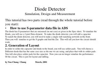
Diode Detector Simulation, Design and Measurement • This tutorial has two parts (read through the whole tutorial before • you start): • How to use S-parameter data file in ADS • The diode has S-parameters that are measured (in our case) or given in the Spec sheet. To simulate the • Diode, you will use a 2-port Data element. To make the diode detector, you will add a capacitor. • To match the diode detector, you will need to make a single stub matching network on the front. • Then you will simulate to get the S-graphs and find the Zin. This will tell you how the circuit should • work. • 2. Generation of Layout • In order to solder the capacitor and diode to the board, you will use solder pads. You will choose a • Different diode that has the same case size as the one we are using, and place that with its solder pads. • You will also place solder pads for the capacitor. Now you can no longer simulate the performance • Of the circuit. This is just for layout and milling. • by You Chung Chung March, 2001
1. How to use S-parameter data files in ADS Designing a diode detector circuit to convert AC to DC voltage
These files are used for Simulation • Use this part of the tutorial to simulate the RF performance of your circuit. You need to include the lengths of all lines (including the pads for soldering elements to). These are found in the layout section, so you will do some back-and-forth between layout and simulation. • Some elements are available in the standard libraries (the cap in this lab), others are not (the diode in this lab). When they are not available, you will have to “create” them using user-defined S-parameters and lines (MLIN). These can come from data sheets (like the HP website) or from measurements (like for this lab).
In the second half of the tutorial, we will do the Layout • “Artwork” is used to define the size and shape of solder connects for components like capacitors, diodes, RF chips, etc. • The dimensions of solder pads (where you actually connect your circuit) are specified on data sheets. They are also available in the libra “library” for many standard elements. • The size of pads add length to your lines, so you will need to include them in your simulation for most accurate results. This means you need to figure out their size before you simulate the circuit, so you will do some back-and-forth between layout and simulation.
1-1. There are two ways to get your S-parameters: • Measure them (most accurate) • Find them on the web or other data sheet (we’d like this to be most accurate, but for this lab it isn’t) • These methods are described below, for your reference. Measured values are given at the end.
1-2. To measure S-parameters of the diode • Build the circuit with just a length of line attached to the device. • Measure the input impedance using the network analyzer. • Compensate for the length of the line to find the S-parameters of your device (Matlab code to do this is included)
1-3. Find the S parameters of your HP diode, Look on this web page:http://www.hp.com/HP-COMP/rf/hprfhelp/products/diodes/hsms285x.htm#s-data
1-4. Copy and Paste the data into a text file (diode.txt). Put this text file into your project directory. S11 (Mag, Phase(degrees))
You may have measured or acquired only the S11 values of a diode. Find the other S-parameters (such as with the included matlab code), and create a text file that has 2-port S-parameters as shown on the next slide. S11 = reflection coefficient S21 = 1+S11 S22 = reflection coefficient (1+j0 for a diode) S12 = 1 + S22 (or in this case, for a diode, it is zero)
1-5. Measured 2-port S-parameters of your diode including the pads:filename is diode2pt.txt !BEGIN ACDATA # GHz S MA R 50.0 !% F n11x n11y n21x n21y n12x n12y n22x n22y 1.75 0.9683 -23.8255 1.9259 -11.7179 0 0 1.0000 0 2.0 0.9683 -29.8098 1.9021 -14.6593 0 0 1.0000 0 2.4 0.9521 -35.1478 1.8610 -17.1282 0 0 1.0000 0 2.6 0.9529 -35.7572 1.8586 -17.4327 0 0 1.0000 0 3.0 0.8956 -44.0234 1.7578 -20.7357 0 0 1.0000 0 !END Copy diode2pt.txt to the data folder in your current project directory.
1-6. Get a Part by typing S2P in the part window & Edit Parameter Double Click on S2P or Edit/Component/Parameter
1-7. Adding Zin block, MLIN, MLOC, MTEE and S2P To make the circuit add MLIN, MTEE, MLOC Also add S parameter and MSub blocks and Zin block to measure Zin. Get s2p 50 ohm lines About 1” Short (1/4-1/2”) To find Zin : Go to Simulation-S_Param and select [S] Zin block
1-8. Simulate your Circuit to find Zin Make this circuit, simulate it and look at the output graph. Zin block Assuming that the values to substitute are calculated.
1-9. Edit C_pad1 Parameter: Define C, W,S,L from the data sheet. Units are from your default.(C_pad1 represents a capacitor WITH its solder pads.) Units here are pF and mils
1-10. Insert S2P parameter file Insert S2P parameter file : Double clock on S2P part and insert parameter file into the File name window. Copy the file into data directory under current working project directory
1-11. Simulate the circuit and look at the graph (Data Display) Add the rectangular plot. Then select “our_zin” to plot from the Plot Traces & Attributes Click Add
1-12. Data Display Select Real part and click ok Again select “our_zin” and click add. Now select Imaginary part and click ok Now click ok in the Plot window
1-13. The Zin Plot, Add markers at 2.4 GHz and 2.6 GHz on both the curves This plot shows the real and imaginary parts of Zin Use these values to design your single stub matching network and also plot on the Smith Chart.
1-14. Add your single-stub network to the circuit Remove the Termination and add your single stub and simulate Use Tune and match to get low S11 in dB
1-15. Data display after simulating Now plot S(1,1) in dB The curve should look like this. You get the matching at the frequency for which you designed your single stub. (2.4GHz) in this case. You should get another curve for 2.6GHz circuit
2. Generation of Layout • You have now simulated how your circuit should work, but you can’t mill it. The mill will not know what to do with the S2P element and won’t leave any particular solder pads for the capacitor. • In this part of the tutorial, you will prepare the circuit to be soldered, but won’t be able to simulate its performance.
Use of Layout • “Artwork” is used to define the size and shape of solder connects for components like capacitors, diodes, RF chips, etc. • The dimensions of solder pads (where you actually connect your circuit) are specified on data sheets. They are also available in the ADS “library” for many standard elements. • The size of pads add length to your lines, so you will need to include them in your simulation for most accurate results. This means you need to figure out their size before you simulate the circuit, so you will do some back-and-forth between layout and simulation.
2-2. Select diode from part library that is the same case size as ours It is under HFDiodeLibrary/High Frequency Diode: di_hit_hsm88as_19930908
2-3. Replace the 2-port data element with the Diode and artwork Assuming that you know where to find the diode MBEND2 can be found under Tlines_Microstrip
2-6. Layout with the diode Ground for extra diode pin Single Stub Matching Network Read VDC here Cap Space Diode Ground You can also plot without the single stub matching network
Remove the Diode • Remove all parts that will be soldered on (diode and capacitor) before saving the file to be milled. • If you don’t, it will “mill” their outline and mess up your board.
2-7. Layout without the DiodeThis is what you should mill. Remember to put the holes for all the shorts(ground, short ckt., stubs, etc) when you mill the circuit
What to turn in • Design two diode detectors, one for 2.4 GHz, and the other for 2.4 GHz. (Slight change in single stub match.) • Print out the layout of your diode detectors, with sizes clearly marked. • Clearly mark where holes for shorts should go (there will be two on each detector).
Question? • If you didn’t “get” something in this tutorial, please tell Dr. Furse or You Chung which slide(s) is confusing. • Thank you!