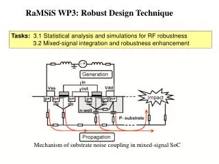
RaMSiS WP3: Robust Design Technique
This report details the advancements made in enhancing the robustness of RF circuits through rigorous statistical analysis and effective noise management. Task 3.1 focuses on the statistical co-design of RF circuits and chip packages, revealing insights from studies on various low-noise amplifier (LNA) designs at 2.5/5.2 GHz. Task 3.2 tackles substrate noise coupling, presenting findings from designed test chips containing both single-ended and differential circuits. These insights aim to mitigate noise interference and optimize circuit performance.

RaMSiS WP3: Robust Design Technique
E N D
Presentation Transcript
RaMSiS WP3: Robust Design Technique Tasks: 3.1 Statistical analysis and simulations for RF robustness 3.2 Mixed-signal integration and robustness enhancement Mechanism of substrate noise coupling in mixed-signal SoC
50 40 (%) 30 Distribution 20 10 A C B 0 14 16 18 20 22 24 26 28 D Yield Gain(dB) WP3 Status on Task 3.1: • RF robustness enhancement through statistical analysis of chip-package co-design of RF circuits • Status: Case studies have been performed on 2.5/5.2GHz LNA design, one manuscript has been completed, which includes • a. Process variation model of IC devices and interconnection parameters • b. Process variation model of RF-chip package technologies • c. On-chip versus off-chip inductors (BPF) trade-offs • d. Statistical analysis and simulations were performed in Agilent-ADS A: Single-chip integrated LNA B: LNA on MCM-D package C: LNA on MCM-C Package D: LNA on MCM-L package
LNA2 LNA1 Noise Sensors VCO1 VCO2 Mixer1 Mixer2 Digital Noise Source WP3 Status on Task 3.2: • Studies of substrate noise coupling to critical RF circuits • Avoid of substrate coupling problem by careful frequency planning of RF circuits and the noise spectrum • Status: • A test chip has been designed and fabricated with both single-ended and differential circuits of LNAs, VCOs, and mixers; on-chip digital noise source and noise sensors are also designed; • Two experiments are in preparation: • a. Measuring the impact of substrate noise coupling to these critical RF circuits; • b. How to push the substrate noise peaks off the working frequencies of these critical circuits by for example allocating different decoupling capacitors