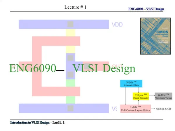
VLSI Design
VLSI Design. smd154 Physical design (back-end). Today’s Topics. Introduction Partitioning Floorplanning Placement Routing. Microelectronic system ASICs System partitioning ASIC floorplanning Placement Routing. A City Buildings City planner Architect Builder Electrician.


VLSI Design
E N D
Presentation Transcript
VLSI Design smd154 Physical design (back-end)
Today’s Topics • Introduction • Partitioning • Floorplanning • Placement • Routing
Microelectronic system ASICs System partitioning ASIC floorplanning Placement Routing A City Buildings City planner Architect Builder Electrician Intro. - Physical design Physical design vs. Building a City
Intro.- History In the beginning… Front-end Team Back-end Team • Logic design (RTL) • Synthesis • Design for test • Floorplanning • Placement • Routing • Physical verification • GDSII
Intro.- History • Smaller geometry + higher gate density results in: • Front-end team and back-end team has to work closer together. • Demand in new design methodologies. • Demand for tools with smaller/faster data structures. Front-end Team Back-end Team
Partitioning Goals • Divide circuit/system into smaller subcircuits/subsystems,called blocks. • Speeds up design process • Can be designed independently • Original system functionality remains intact • Simplifies routing task • May degrade performance Objectives • Minimize Interconnections Between Blocks (mincut problem) • Minimize delay due to partitioning. Constraints • Area (not so important on chip level) • Number of terminals (depends on area) • Number of blocks (depends on capacity of placement algorithm)
Partitioning Partitioning Algorithms Mincut problem is NP-complete! Group Migration Algorithms • Start with some (usually random generated) partitions and move components between blocks to improve results. • Quite efficient. Simulated Annealing/Evolution Algorithms • Carry out partitioning by using a cost function. • Computationally intensive compared to other methods.
Partitioning 1 2 3 4 5 6 7 8 1 5 8 4 2 6 3 7 Initial Bisections Cutsize = 9 Final Bisections Cutsize = 1
Partitioning After circuit partitioning phase • Area occupied by each block can be estimated • Possible shapes of blocks can be ascertained • Number of terminals required by each block is known • Netlist specifying connections between blocks is available Next step: Floorplanning
Floorplanning Goals • Assign shape and location of blocks. • Decide location of I/O pads. • Decide location and number of power pads. • Decide type of power distribution. • Decide location and type of clock distribution. Objectives • Keep highly connected blocks physically close to each other. • Minimize chip area. • Minimize delay.
Input Set of blocks. Area estimation. Possible block shapes. Number of terminals. Netlist. Output Shapes (Area & Aspect Ratio) and locations of blocks. Floorplanning • Soft Blocks • Flexible shape • I/O positions not yet determined • Hard Blocks • Fixed shape • Fixed I/O pin positions
Block 4 Block 3 Block 2 Block 1 Floorplanning Aspect Ratio Bounds No Bounds With Bounds lower bound ≤ height/width ≤ upper bound NOT GOOD!! Soft Blocks Hard Blocks
Floorplanning Design Styles Full Custom • Floorplanning is needed. Standard Cell • Fixed cell dimensions. Floorplanning translates into a placement problem. • Floorplanning may be required for large cells if they are partitioned into several blocks. Gate Array • Placement problem.
Floorplanning Optimize Performance • Chip area. • Total wire length. • Critical path delay. • Routability. • Others, e.g. noise, heat dissipation. Cost = αA + βL, A = total area, L = total wire length, α and β constants.
Floorplanning Area Deadspace Minimizing area = Minimizing deadspace • Wire length estimation • Exact wire length not known until after routing. • Pin position not known. • How to estimate? • Center to center estimation.
Floorplanning Floorplanning methods • Constraint Based. • Linear Programming. • Mixed Integer Linear Programming (MILP) -> NP-complete. • Rectangular Dualization Based. • Hierarchical Tree Based. • Simulated Annealing and Evolution Algorithms. • Timing Driven.
Floorplanning Simulated Annealing Algorithm. • Represent floorplan by normalized polish expression. V V H H H 3 4 H 7 2 5 1 6 7 5 4 6 2 3 1 E = 16H7H25HV34HV
Floorplanning Try to optimize cost by moving blocks around. M1 : Swap two adjacent operands. M2 : Complement some chain. M3 : Swap adjacent two operand and operator. cost = αA + βL 1 1 1 1 M1 => M3 => M2 => 2 4 5 4 5 5 5 3 2 3 4 3 2 4 3 2 34V2H5V1H 32V4H5V1H 32V45HV1H 32V45VH1H
Placement Goals • Arrange all logic cells within the flexible blocks. Objectives (Ideally) • Guarantee the router can complete the routing step. • Minimize all critical net delays. • Make chip as dense as possible. • Minimize power dissipation. • Minimize cross talk between signals. Ideally objectives are difficult to define for use in algorithms and even harder to actually meet ...
Placement Objectives (Compromised) • Minimize total estimated interconnect length. • Meet timing requirements for critical nets. • Minimize interconnect congestion. Problems • No point in minimizing the interconnect length if we create a placement that is too congested to route! • Trying to minimize both interconnect congestion and interconnect length may result in long interconnection delays between some logic cells.
Placement Placements Algorithms • Constructive Placement • Uses a set of rules to create a constructed placement • Interative Placement • Take an existing placement and improve it for each iteration Min-Cut Placement method 1. Cut placement area into two pieces 2. Swap logic cells to minimize cut cost 3. Repeat process from step 1, cutting smaller pieces until all logic cells are placed
Routing is to connecting pins with wires a NP-hard problem Constraints Minimize total wire length Minimize knees in path Meet timing budget Steiner Tree The optimal routing path is a Steiner Tree Finding a Steiner Tree is a NP-complete problem Types Maze routing Channel routing Switchbox routing River routing (Single layer) Global Routing Doesn't make any connections only plans them. Decides which channels is going to be used for routing Marks channels with wire accommodate capacity Detailed Routing Connects pins and pads, creates vias. Special Routing Clock routing Routing
Routing Obstructions • Areas that can only be crossed on a certain layer. Obstacles • Areas that can’t be crossed on any layer, have to route around. Channel • Rectangular area with connection points on two sides. Switchbox • Area with connection points on four sides. Channel Switchbox
Routing Lee-Moore (Maze routing) -Guaranties to find the shortest path between two nodes if it exist, but it only holds for one net. -Demo http://foghorn.cadlab.lafayette.edu/cadapplets/MazeRouter.html The Left Edge Algorithm (Channel routing) -No guarantee to success. -Makes global considerations, often resulting in better routing then maze. -Demo http://foghorn.cadlab.lafayette.edu/cadapplets/ChannelRouter.html
Routing Clock and Power routing • A part of floorplanning CLOCK • Asynchronous/synchronous system • Clock skew and delay needs to be considered. POWER • Low resistance in metal line need to be considered. • Power and GND is routed in separate nets.