PCI-E X4 Status Report for FPGA 780 Pin Board with Embedded Transceivers
Report on the status of a PCI-E X4 board with FPGA 780 pin configuration, controlled impedance, and DDR2 compatibility. Detailed information on board mounting, interconnections, and trigger architecture. Strategy for LKr trigger implementation using existing TELL1 board and optical transceivers. Throughput estimation and considerations for halo expansion with TELL1.

PCI-E X4 Status Report for FPGA 780 Pin Board with Embedded Transceivers
E N D
Presentation Transcript
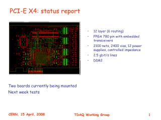
PCI-E X4: status report • 12 layer (6 routing) • FPGA 780 pin with embedded transceivers • 2100 nets, 2400 vias, 12 power supplies, controlled impedance • 2.5 gbit/s lines • DDR2 Two boards currently being mounted Next week tests
Fit results with quartus 18k Logic Elements available for the user
Parameters • LKr readout (depending on readout implementation) • CTP interface (the board can act as a CTP coprocessor: 18k Logic Elements free) • TELL1 readout • PCI-E - 4 lines – 16 bit @ 125 MHz (2.0 gbit/s) per lane • Optical link – 4 TLK2501 – 16 bit @ 75-125 MHz (1.2-2.0 gbit/s) • Copper link – 2-4 DS90CR485 – 48 bit @ 66-133 MHz (3.1-6.3 gbit/s) – maximum working frequency depends on cable length Can be used for
LKr trigger proposal Assumptions: • 216 LKr readout boards (64 channels per board) • Digital sum on 4x4 cells on the readout boards Trigger concentrator boards • Receives 16 readout boards • Peak finding in space and time • Pulse reconstruction with 1-2 ns time resolution • Trigger primitives sorting and propagation to CTP
1 1 16 1 16 1 LKr Trigger: architecture 1st layer Trig board: cluster reconstrtrig prim gener RO board (CERN): digitization + RO4x4 ch digital sum 2nd layer Trig board: sortinginterface to CTP 216 x 16 x 1 x RO board(CERN) Trigger board Trigger board CTP 4 ch 64 ch 1024 ch • 16 optical input • 1 optical output • 9U x 400 mm
LKr trigger: implementation • The best solution would be to design a completely new system • A good compromise is to use the existing TELL1 board as a motherboard and design only the interconnections (implemented with TLK2501 + optical transceiver) • TELL1 was designed some years ago with (now) old components • TELL1 exists and is working • We know it (working on LHCb TELL1 muon firmware) • We already used TLK2501 + optical txrx in an R&D project OUR STRATEGY Design a prototype LKr trigger with TELL1 and all the interconnect implemented with TLK2501 + optical transceiver (to minimize design effort).Once it works, if we have time and if needed start the design of the new motherboard
Throughput estimation • 30 MHz istant/13k cell ~ 150 kHz/board -> average! • Our conservative assumption is 10 x average in the central region = ~ 1.5 MHz/board • 16 bits x 4 pads x 8 samples @ 1.5 MHz = ~ 800 Mbit -> we can work with 4x4 pads and a TLK2501!
TELL1 board 24 optical input
How can we perform halo expansion with TELL1? • If we work without halo expansion -> 1 optical link for RO card, up to 24 optical input on the trigger concentrator (TELL1) • If we want halo expansion on the TELL1 we can try the following approach:each RO card equipped with 1 optical link + 8 lemo out + 8 lemo in cables -> if a seed is found in a RO card one or more neighboring RO cards are flagged for transmission24 TELL1 input arranged as 16 input + 4 bidirectional links (halo expansion between two different TELL1s) to be checked!
Why to design a new board? Pulse time reconstruction is a typical DSP application Altera Stratix III (E version) with embedded DSP