Download
1 / 36
360 likes | 395 Vues
Explore selective deposition, lithography, post-exposure bake, and sensor technology for optimal semiconductor manufacturing processes. Discover the integration of temperature and heat flux sensors to enhance process control and improve yield rates.

E N D
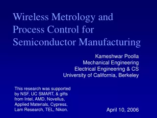
Wireless Metrology and Process Control for Semiconductor Manufacturing Kameshwar Poolla Mechanical Engineering Electrical Engineering & CS University of California, Berkeley April 10, 2006 This research was supported by NSF, UC SMART, & gifts from Intel, AMD, Novellus, Applied Materials, Cypress, Lam Research, TEL, Nikon.
semiconductor manufacturing background
What is it? • Selective deposition & selective removal of various materials to form ICs • Selectivity is done by protecting desired areas with resist IBM Power PC750
Lithography • Spin-coat Resist • Cr Mask • Expose • Post Exposure Bake • Start with a Si wafer • Develop • Etch or Deposit
Process Overview Photomask Scanner PEB PAB Etch Develop Resist PDB Track Production Wafer Flow
Critical Dimension (CD) • Captures quality of pattern transfer • CD Target – desired width of printed lines • CD(x,y) – actual width of printed lines • Depends on (x,y) because process varies across wafer • Measured on test wafers using CD SEM or Scatterometry
CD means μ and spreads σ • Want CD Mean at Target • small CD means faster switching speeds • CD spread Across wafer & wafer-to-wafer • small CD spread can use aggressive design rules higher device density better binning yields
Bad Good
6nm Bin 1 $ Bin 2 Device/Fab Economics Bin 3 Binning 11nm Typical CD Distribution Target CD Post OnWafer Optimization Intel P4 Prices: 3.8 GHz - $429 3.2 GHz - $336 2.8 GHz - $279 Yield Yield Improved Yield & Bin Sort = $$$
Post Exposure Bake • Key step – greatly influences CD μ and • Makes exposed resist diffuse • To reduce standing wave patterns • Gives better pattern transfer • Must be very accurately controlled • State-of-the-art ±0.3 ºC across 300 mm wafer
PEB reduces Standing Waves Courtesy of CNF, Cornell University
Our Plan ~1997 • Decided to do Control of Lithography • Feedback Control requires Sensors & Actuators • Available Actuation? Plenty – exposure dose, focal plane, PEB Temp • Available Sensors in Lithography? Not many and pretty useless for control
processing equipment finished wafer Need in situ Sensing What was the state of the wafer during processing? wafers to be processed
in situ Sensing • Need wafer-state information • Temperature in post-exposure bake • Latent image in lithographic exposure • Etch rate of wafer in plasma etch • Deposition rate in CVD processes • The Big Problems • Chamber access • Deployment cost
Solution: SensorWafers In-situ sensor array with integrated power and telemetry
processing equipment SensorWafer data feedback process control wafers to be processed base station The Approach
Temperature Sensors • Useful for PEB, plasma etch, implant • Objectives Monitor wafer temperature at 4 locations (within 1ºC) • Design • Off-the-shelf temperature sensor modules • PIC microprocessor (with integrated 4 channel A/D) • Infrared data transfer (IrDA compliant) • Error detection (CRC-16)
Batteries P Ir-LED Batteries P Sensor Ir-LED Sensor Early attempts … Problems: clearance, isolation, contamination & they are ugly !
I I Poly-Si V Etch Rate Sensor • Sensor to measure polysilicon etch rate • Based on van der Pauw probe electrical film-thickness measurement:
Results Problems: clearance, isolation, contamination
Thermal Flux Sensors • Plasma etch is highly sensitive to wafer temp etch rate, selectivity, and anisotropy • Heat delivered to the wafer has two sources • Ion flux bombardment Indirect measure of physical etch • Exothermic chemical etch reactions Indirect measure of chemical etch • Want to resolve these heat fluxes • Can deduce sidewall, anisotropy etc.
Incident heat flux (q ) Dielectric, thermal conductivity Temperature Sensors t Heat flux sensor design • Simple, layered heat flux gauge • Not enough sensitivity
Incident heat flux T Antenna Antenna Base Membrane Make the Heat Travel Far
T b Incident heat Heat flow T Antenna / Membrane Structure Membrane Top View D Heat flow within thin dielectric membrane Membrane Side View Heat sink Heat sink
Heat Flux Resolution • Discrimination between physical and chemical sources • Use two heat flux sensors: one exposed, one covered • Exposed sensor is heated by both sources • Covered sensor receives only physical heating
PR Al SiO2 poly Si Si3N4 Design #1 • Membrane: Silicon nitride • Antenna: SiO2 / Aluminum • Plasma-etched material: resist (O2 plasma) • Temperature sensors: polysilicon • Tethered power and communication Heat sink Heat sink
Layout – Wheatstone Bridge Etched Sensor Non-Etched Non-Etched
Layout – Full Die (20 per wafer) Sensors Edgeboard Connector
PR poly poly Si Si3N4 Design # 2 • Antenna: Undoped polysilicon (low ) • Linewidths: increased • Tethered power and communication Heat sink Heat sink
heater sensor off-the-shelf sensor Testing • Test sensors on the “bench” • Use an off-the-shelf heat flux sensor and a heating element to compare readings: Aluminum heat sink vacuum chamber
Going up the food chain • Sensors become rapidly commodified • Value is in using the data • This is through Control, Modeling, Optimization • Examples • Equipment Control • Fault Detection and Isolation • Process Optimization
The Value ofControl • PEB Example • Control spatial temperature of bake plate • Yesterday ± 0.3 °C • Today ± 0.15 °C • Result: 1 nm reduction in CD spread • Benefit: mid-sized fab in 1st year of product lifecycle ~$3/die * 200 die/wafer * 20,000 wafer/mon * 12 mon/yr • 144 M$ per year !!