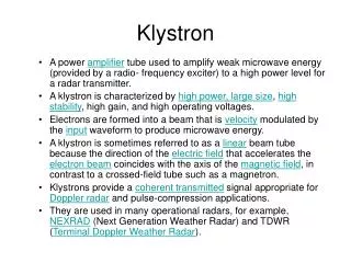
Download
1 / 27
270 likes | 339 Vues
Learn about the design proposals, R&D progress, and future strategies for developing high-energy efficient klystrons. Explore key collaborative efforts and innovative methods to achieve breakthrough efficiency levels in RF power sources.

E N D
CEPC650MHz High Efficiency Klystron R&D Zusheng ZHOU(周祖圣) RF Power Source Group Accelerator Division, IHEP May. 4, 2016
Contents ■Present situation ■Design proposal ■R&D Progress ■Summary
Present situation The RF relevant FCC and CEPC machine parameters have well converged – they clearly indicate the need for Higher Energy Efficiency.
Present situation • 2014 saw a breakthrough in klystron theory: • The “congregated bunch” concept was re-introduced [V.A. Kochetova, 1981] (later electrons faster when entering the output cavity). • The concept of “bunch core oscillations” was introduced [A. Yu. Baikov, et al.: “Simulation of conditions for the maximal efficiency of decimeter-wave klystrons”, Technical Physics, 2014] (controlled periodic velocity modulation) • The “BAC” method was invented [I.A. Guzilov, O.Yu. Maslennikov, A.V. Konnov, “A way to increase the efficiency of klystrons”, IVEC 2013] (Bunch, Align velocities, Collect outsiders) • These methods together promise a significant increase in klystron efficiency (approaching 90%) • An international collaboration has started – prototypes are being designed. (SLAC plans to convert an existing 5045 klystron– simulations are encouraging)
“Bunch core oscillations” explained 2 “Classical” bunching RF=78.0% RF=78.0% particle phase Normalised velocity Useful RF phase Output cavity 0 RF period, rad 2 Useful RF phase New bunching method with core oscillations RF=89.6% Normalised velocity particle phase Normalised velocity Output cavity 0 RF period, rad
HEIKA collaboration • HEIKA – “High Efficiency International Klystron Activity” is evaluating and implementing this “breakthrough”. • HEIKA Members: Labs (CERN, ESS, SLAC, CEA), Universities (MFUA, Lancaster), Industry (Thales, L3, CPI, VDBT) • It studies theoretically and experimentally high efficiency klystrons for both pulsed (e.g. CLIC, ESS) and CW applications (FCC). I. Syratchev (CERN), A. Baikov (MFUA), I. Guzilov (VDBT), J. Neilson, A. Jensen (SLAC), G. Burt, D. Constable, C. Lingwood (U Lancaster), A. Mollard (CEA), R. Marchesin (Thales), Q. Vuillemin (Thales/CERN), C. Marrelli (ESS), R. Kowalczyk (L-3com), (Toshiba), T. Grant (CPI)
Collider RF power source Klystron key design parameters
实施途径 速调管效率提高主要通过以下途径: (1)低导流系数电子枪 (2)采用高次谐波腔 (3)采用多注速调管 (4)利用降压收集极 (5)束团内核振荡(COM)方案,比如BAC (Bunch Alignment Collector)方法 (6)绝热群聚方法 (7)Congregated bunch concept 目前低导流系数和高次谐波腔组合、低导流系数和多注的组合技术成熟,速调管效率65%以上。 要实现极高效率(80%以上)通常需要多种方法的组合,CEPC速调管将采用方案以下两种方案: (1)单注低导流系数和高次谐波腔组合,理论模拟效率72%以上。 (2)单注低导流系数和BAC组合,期望效率高于80%。 CEPC速调管为CW速调管,功率较低,即使在低导流系数下电压也不算太高,因此可先采用较为简单的单注速调管,多注速调管可同步进行模拟设计。
Klystron Schedule and strategy Because of klystron efficiency is more than 80%, in order to fulfill this program, there may have following problems: we (China) have not an experienced to manufacture the high power, UHF klystrons. There is not the big furnace infrastructure in China also. Design and simulation are not enough and matured, therefore we need to step up one by one. Let’s start from beam tester, classical design and currently progressed design such as HEIKA. In order to save the money and time, demountable structure is another way.
Klystron Schedule and strategy(2) • Merits • Saving the money • Saving the time • Possible to try 2 or 3 designs (1) Beam tester (2) #1 prototype (3) #2 prototype
Klystron Concept Design Rough Parameters Parameters for Electron optics Parameters for interaction region calculation
Electron Gun Design and Simulation Egun simulation result: Area compression ratio : 4.4 Perveance: 0.647μP Cathode current density:0.39A/cm2~0.43A/cm2 Max. electric field : 2.520kV/mm Cathode current density -57kV -81.5kV 0kV Gun region beam trajectory simulation with Egun Electrode E fied density optimization with Possion
Electron Optics Design and Simulation Laminar flow,Beam ripple <5.2% whole tube beam trajectory simulation with EGUN Magnetic field density of Brillouin Flux :107.5 Gauss Magnetic field density at cathode: 41 Gauss Magnetic field density at tube body: 200Gauss K=0.75
Gun Assembly Design Basic drawing of gun assembly using Auto Inventor. Geometry is come from the POISSON calculation. Purpose is determine the ceramic sealing structure. And size to order to the company. Based on this first drawing, this will be revised by IHEP Mechanical Group to more complete drawing Currentstageofdrawing
Gun Assembly Design(3) In order to study gun assembly problems, several problems occurred at the HV ceramic due to the multipactor are planed to be analyzed. Those are simulated by POISSON and CST, and in order to make clear the geometry, basic drawings.
Collector Design and Simulation • Collector shape and beam dissipation optimization Jcollector optimization using universal beam spread curve collector optimization using EGUN code Crosscheck of beam trajectory with EGUN and MAGIC
Collector Design and Simulation(2) Groove dimensions optimization Contour of temperature and water pressure loss
Collector Design and Simulation(3) Collector Thermal analysis Groove structure for 2 meter tapered collector in Ansys-CFX contour of temperature on inner surface of copper domain contour of temperature of water domain
Collector Design and Simulation(4) • Collector geometry of tapered part 2030mm A B C D E Geometry of collector tapered part
Cavities design and optimization Optimize cavity geometry to get the desired characteristic parameters and high R/Q. TM010 electromagnetic field pattern Table 1 Cavity geometry and characteristic parameters
Cavities design and optimization(2) Total power gain57dB -3dBbandwith:643MHz~658.4MHZ
Current Status -Beam tester Concept Simulation • Gun • HV Seal • Collector • Drawing Gun HV Seal Drawing Collector drawing will be proceeded
Current Status -Beam tester Latest drawing of Beam test stand
Summary • Complete gun design • Order the cathode and ceramic • Complete the collector design • Complete the designing / drawing and start manufacturing • In order to do the quick manufacturing, parallel schedule for manufacturing and cathode manufacturing and processing • Furnace problem There is no big furnace in China, we are looking for appropriate company to build it.