
VLSI ASIC Logic-analyzer Interface Design
E N D
Presentation Transcript
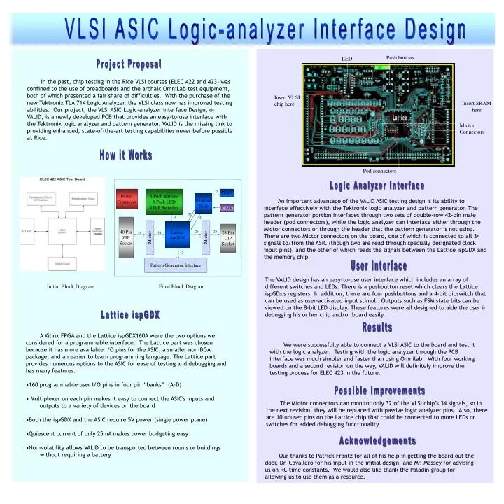
VLSI ASIC Logic-analyzer Interface Design Push buttons LED Project Proposal sexy In the past, chip testing in the Rice VLSI courses (ELEC 422 and 423) was confined to the use of breadboards and the archaic OmniLab test equipment, both of which presented a fair share of difficulties. With the purchase of the new Tektronix TLA 714 Logic Analyzer, the VLSI class now has improved testing abilities. Our project, the VLSI ASIC Logic-analyzer Interface Design, or VALID, is a newly developed PCB that provides an easy-to-use interface with the Tektronix logic analyzer and pattern generator. VALID is the missing link to providing enhanced, state-of-the-art testing capabilities never before possible at Rice. Insert VLSI chip here Insert SRAM here Lattice Mictor Connectors How it Works Pod connectors Logic Analyzer Interface Power Connector 4 Push Buttons 8 Pack LED 4 DIP Switches 2 JTAG An important advantage of the VALID ASIC testing design is its ability to interface effectively with the Tektronix logic analyzer and pattern generator. The pattern generator portion interfaces through two sets of double-row 42-pin male header (pod connectors), while the logic analyzer can interface either through the Mictor connectors or through the header that the pattern generator is not using. There are two Mictor connectors on the board, one of which is connected to all 34 signals to/from the ASIC (though two are read through specially designated clock input pins), and the other of which reads the signals between the Lattice ispGDX and the memory chip. External PLD Clock 32 16 2 40 Pin ZIF Socket Lattice ispGDX 28 Pin DIP Socket 26 26 34 34 Mictor Mictor 42 Pattern Generator Interface User Interface The VALID design has an easy-to-use user interface which includes an array of different switches and LEDs. There is a pushbutton reset which clears the Lattice ispGDx's registers. In addition, there are four pushbuttons and a 4-bit dipswitch that can be used as user-activated input stimuli. Outputs such as FSM state bits can be viewed on the 8-bit LED display. These features were all designed to aide the user in debugging his or her chip and/or board easily. Initial Block Diagram Final Block Diagram Lattice ispGDX Results • A Xilinx FPGA and the Lattice ispGDX160A were the two options we considered for a programmable interface. The Lattice part was chosen because it has more available I/O pins for the ASIC, a smaller non-BGA package, and an easier to learn programming language. The Lattice part provides numerous options to the ASIC for ease of testing and debugging and has many features: • 160 programmable user I/O pins in four pin “banks” (A-D) • Multiplexer on each pin makes it easy to connect the ASIC's inputs and outputs to a variety of devices on the board • Both the ispGDX and the ASIC require 5V power (single power plane) • Quiescent current of only 25mA makes power budgeting easy • Non-volatility allows VALID to be transported between rooms or buildings without requiring a battery We were successfully able to connect a VLSI ASIC to the board and test it with the logic analyzer. Testing with the logic analyzer through the PCB interface was much simpler and faster than using Omnilab. With four working boards and a second revision on the way, VALID will definitely improve the testing process for ELEC 423 in the future. Possible Improvements The Mictor connectors can monitor only 32 of the VLSI chip’s 34 signals, so in the next revision, they will be replaced with passive logic analyzer pins. Also, there are 10 unused pins on the Lattice chip that could be connected to more LEDs or switches for added debugging functionality. Acknowledgements Our thanks to Patrick Frantz for all of his help in getting the board out the door, Dr. Cavallaro for his input in the initial design, and Mr. Massey for advising us on RC time constants. We would also like thank the Paladin group for allowing us to use them as a resource.