Download
1 / 33
340 likes | 436 Vues
This proposal outlines a collaborative research project between the Electrical Engineering Division, CU Engineering Department, and Zeiss SMT to advance photonics and electronics technologies. The collaboration aims to leverage industry expertise, create valuable intellectual property, and secure government support for cutting-edge research. Key stakeholders include strategic partners from the electronics, photonics, and materials sectors. The project's mission is to drive multidisciplinary research to develop innovative materials, components, and systems for future technology platforms.

E N D
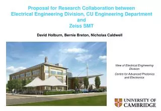
Proposal for Research Collaboration between Electrical Engineering Division, CU Engineering Department and Zeiss SMT David Holburn, Bernie Breton, Nicholas Caldwell View of Electrical Engineering Division Centre for Advanced Photonics and Electronics
The Centre for Advanced Photonics and Electronics (CAPE) – ---- is an exciting new venture based around world-leading facilities and expertise at the University of Cambridge. Supported and guided by a small number of strategic industrial investors, representing the global supply chain in this sector, the centre will lead to a new form of joint university-industry research that is leading edge, vertically integrated and commercially relevant. In January 2006 the Electrical Engineering Division moved into the new CAPE Building What is CAPE?
Centre for Advanced Photonics and ElectronicsCAPE(Electrical Engineering) Electronics & Photonics Research within the Engineering Department
The CAPE Project CAPE Director Professor Bill Milne Head of Electrical Engineering CAPE Chairman Professor Bill Crossland Cambridge University Engineering Department
How is the vision to be achieved? • A small number of strategic partners, reflecting the supply chain in the sector, are investors in CAPE. Others may join later • Steering committee involving strategic partners and key academics will set the research agenda for CAPE • Direct day-to-day collaboration through embedded researchers and exchange of personnel • Expertise of strategic partners to support commercial exploitation • Creation of facilities to support technology to proof of concept devices • Creation of valuable IP for the benefit of all strategic partners • Leverage involvement to secure significant government (UK and EU) support
The Vision CUED CAPE Dow Corning Alps Electric Industries Solid State Electronics & Nano-scale Science Marconi plc Electronics, Power & Energy Conversion Others Photonics Sensors & Opto-Electronics
Materials Core Competencies Product Technologies LC Cell & Flat Panel Displays Liquid Crystals LCOS Adaptive Optics Wafer Processing Silicon/IIIV-based materials Planar Light-wave Circuits Nano-scale Technology Si/IIIV micro- & opto- electronics Carbon-based materials Packaging MEMS Design & Modelling Photonic Crystals
CAPE Mission To invent and develop, through multidisciplinary research, materials, processes, components and systems; define the future strategy and market implementation; and set the industry agendas for the convergence of photonic and electronic technology platforms
CAPE will: • emphasise rapid application of breakthrough research by placing issues of industrial importance at the top of the research agenda; • provide a focal point for contributing companies to form strategic relationships at an early stage involving directed R&D; and • provide a focus for multidisciplinary research involving engineers, but also chemists, physicists, materials scientists and bioscientists.
Proposal for Research Collaboration between Electrical Engineering Division, CU Engineering Department and Zeiss SMT David Holburn, Bernie Breton, Nicholas Caldwell
Zeiss SMT • The major player in the market • Enhance products through innovation • Cost of research • Collaboration with academia • A cost-effective mechanism
Track Record • Department achieved highest possible 5*A rating (international and national excellence in all areas of research). • Research on SEM dates back to 1948 • Continuous activity during intervening period • “50 years of SEM” in December 2004 • Many developments in last ten years
Track Record (2) • Web-based technologies, providing new opportunities in remote diagnosis – NETSEM • SEM fault diagnosis – First A.I.D. expert system • SEM ease of use – XpertEze expert system • Electron source management • Automated filament saturation (AutoSat), Filament lifetime monitoring • Beam profile determination • Software algorithms: • gun alignment, focusing, dynamic noise reduction, astigmatism • Neural networks for particle analysis of wear debris
Other activities • Academic publications • International conferences • MSA, Scanning, EUREM • RMS Micro • Computers in Microscopy, CAMSEM • Advanced Image Processing • Advances in Imaging and Electron Physics • Sir Charles Oatley and the Scanning Electron Microscope", Breton, B.C., McMullan, D., & Smith, K.C.A., Volume 133, Elsevier Academic Press, 2004 • 50 years of SEM
Research Proposals • Intelligent Microscopes • Service Support Tools for SEM and TEM • Improvements in Electron-Optics Control • Novel Stereo Techniques & Intelligent Stereo • JITS (“Just In Time Scanning”) Microscopy • Manipulation of Nanoscale Objects in the SEM • Extension of image processing capabilities
Intelligent Microscopes • Extend XpertEze to Zeiss instruments • Knowledge bases for special applications • Case-based/knowledge database • Embedded implementation • E.g. XML, callable from VB, VC.
Service Support • Deployment of service support tools • On-line searchable database • Further development of First A.I.D. expert system • Software extensions for newer Zeiss microscopes • Direct savings in technical support • Improved service through better fault diagnosis
Control of Electron-Optics • Novel algorithms and advanced auto-functions for SEM electron-optics • In LaB6 guns, control of: • Focus • Astigmatism • Saturation • Extend to wider range of sources
Intelligent Stereo Techniques • Stereo – still relatively unexploited in the SEM • Visually attractive images • Valuable specimen depth information • Current implementations limited to specific columns • Difficult user interface • Restricted uptake of the technique. • Propose: • new techniques for use with conventional, VP & FE instruments • intelligent software ‘wizards’ - eliminate black art nature of stereometry
‘Just In Time Scanning’Microscopy • Biological applications • Uncoated and fragile samples • Operator has limited time-frame • Otherwise • charging • beam damage becomes excessive. • Propose: “just-in-time scanning” techniques • to reduce damage • extend the operator’s window of opportunity.
Manipulate Nanoscale Objects in SEM • Nano-assembly/manipulation increasingly important • characterisation of objects • building prototype devices • Picking up small objects: • organic nanowires, • cells, • laminar slices
Manipulate Nanoscale Objects (2) • Place on electrodes/grids for characterisation. • Objective: control object movement in SEM • demonstrate nanomanipulation • measurement of material characteristics
Manipulate Nanoscale Objects (3) • Three strands • Hardware development • 3D nanomanipulator • Visualisation of the environment • 3D model of manipulator and target • Software development • Sense manipulator coordinates using stereometry and autofocusing • Communication • Calibration • Automated manipulator control
Extended image processing capability • Need for efficient real time image processing • Traditional architecture • Single CPU • Responsible for control of the instrument • Monitoring activities • User interface. • Multi-processor PC architectures • Potential to optimise time-consuming tasks • Fourier transforms, • spatial filters, • deconvolution, • correlation, • neural nets
Other Research Applications of SEM • Immense importance to Electrical Division • Need to compete for instruments elsewhere • Ongoing projects • Inspection of carbon fibres • Examination of ink/bubble jet print heads and media • Quality control of lithographic processing • Examination of semiconductor devices • smart power, high voltage • Inspection and operation of • micromachined cantilevers, • accelerometers and • other transducers and assemblies • Inspection of optical devices, fibres and couplers • Development of lithography based on contamination • QC for fabrication of carbon nanotube materials & structures
Teaching Applications of SEM • Need for instrument to serve teaching needs 4B7 VLSI Design, Technology and CAD (20) • Practical SEM sessions: approx 2 hours in groups of 3-5 4B6 Solid State Devices (20) • Elucidation of device structures 3B2 Integrated Digital Electronics (80) • SEM micrographs to indicate IC structures Part IA Linear Circuits and Devices (300) • provision of SEM micrographs to illustrate device structures;
IP and Confidentiality • Contracts negotiated with • Sponsors • Principal Investigator • CAPE Steering Committee • Strategic Partnership Agreement (SPA) • signed by the University and the Strategic Partners • Terms govern handling of IP arising from the Project • licensed, exclusively or non-exclusively, to Sponsor • assigned to the Sponsor, (revenue-sharing agreement) • placed in the public domain • Employment contracts bind: • University Members • Strategic partner employees • Students sign confidentiality document
Project Review • Regular reports to Sponsor on project progress • Typically, brief 6-monthly written reports • Final written report within 3 months of expiry/termination • Probability of patentable/exploitable innovations • emphasis on accurate record-keeping • numbered laboratory notebooks • Opportunities to showcase premier products • Integral to collaboration under CAPE. • Regular visits by CUED personnel to Zeiss • review and discussion • technical assistance. • Invitations to Zeiss personnel to visit CUED • collaborative planning sessions and interaction with projects
Project Team • David Holburn – PI Subject to availability of supporting funding: • Bernie Breton – experienced advice/support (part-time) • Nicholas Caldwell – key software developments (part-time) • Research Students will undertake projects under • CAPE contracts, • EPSRC studentships, • other awards • Projects offered to fourth-year M.Eng students
Thank you for your attention David Holburn, Bernie Breton, Nicholas Caldwell View of Electrical Engineering Division Centre for Advanced Photonics and Electronics
Centre for Advanced Photonics & Electronics (CAPE)Electrical Engineering DivisionProf.W.I.MilneGrouped into 3 main Areas