Download
1 / 55
550 likes | 623 Vues
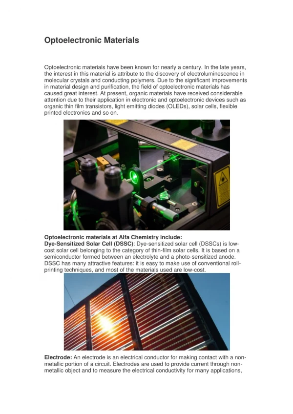
This textbook provides an introduction to the principles and practices of optoelectronics and photonics, covering topics such as band gaps, carriers, doped materials, equilibrium distribution of carriers, and minority carrier lifetimes.

E N D
Fundamentals of Optoelectronic Materials and Devices 光電材料與元件基礎 Hsing-Yu Tuan (段興宇) Department of Chemical Engineering, National Tsing-Hua University
Textbook in this lecture • Optoelectronics and photonics priciples and practices, S.O. Kasap 1999 • Solid state electronic devices, Ben G. streetman and sanjaybanerjee, fifth edition
Distinction between insulator, semiconductor and metal Insulator Semiconductor Metal conduction band plenty of electrons > 5 eV valance band -few electrons excited to conduction band Ex, Si: 1010 / cm3 (note: Si has 5x10²² atoms/cm3) -very few electrons excited to valance band at room temperature Streetman p62
Semiconductor, band gap, and wavelength The band gap corresponds to the wavelength of light that emits from the semiconductor Eg=1240/λeV
Carrier: electron and hole • Some electrons were excited to the conduction band at temperature >0K • For convenience, an empty state in the valence band is referred to as a hole • Electron-hole pair (EHP): conduction band electron and the hole are • created by the excitation of a valence band electron • -EHPs are free charge carriers in semiconductor materials • -Si, at room temperature has 1010 EHP/cm3 (Si: 5x10²² atoms/cm3)
Doped materials Donors: P, As, Sb (Column V elements ) , n-type, provide one additional electron Acceptors: B, Ga, In, (Column III elements), p-type provide one additional hole n p P+ B- - -weakly bound -bonding strength EB~ 0.05 eV (Si bonding ~1.12 eV) The nomination is not limited to Si, but for any semiconductors Majority carrier - electron in a n-type material hole in a p-type material Minority carrier – hole in a n-type material electron in a p-type material
Equilibrium distribution of carriers in intrinsic and doped semiconductors hole 1-f(E) Ec Ei Ev i Intrinsic n fermi level shift Ec EF Ei Ev Ec Ei EF Ev p p-type n-type g(E)
R-G statistics • A technical men given to the mathematical characterization of recombination-generation process • R-G evaluates the time rate of change in the carrier concentrations -The rate of change in the carrier concentration n~no perturbation Ec ET(R-G)censter Ev △P △p<<no n-type semiconductor Low level injection implied △p<<no n~no in an n-type material △n<<Po p~poin an p-type material
n-type semiconductor after a perturbation perturbation perturbation t=0 t>0 t->infinite P0 △P △P=0 n-type semiconductor n-type semiconductor n-type semiconductor The change of minority carriers dominate the recombination rate To be approximately Proportional to NT (R-G center numbers) (R-G) (since the multitude of electrons rapidly fill any level that is vacant) n~no Ec EF ET(R-G)censter Ev To be approximately Proportional to △P (R-G) • The more holes available for • annihilation, the greater • the number of holes recombining • per second. po △P<<no For holes in a n-type material; (R-G) For electrons in a p-type material (R-G) Cp Cn is a positive proportionality constant
Minority Carrier lifetimes We introduce the time constants For holes in an n-type material (R-G) For electrons in an p-type material (R-G) -are called minority carrier lifetimes ; interpreted as the average time an excess minority carrier will live in a sea of majority carriers -In a Si with very few R-G center, lifetime is around 1 msec - Typical minority carrier lifetimes in most Si device is around 1 μsec Diffusion lengths electron in a p-type material hole in an n-type material
Charge neutrality • In a semiconductor with equilibrium state. the charge should be neutral, otherwises, there occurs an electric field - qp – qn + qND - qNA= 0 + Charge/cm3 ND+ = number of positively charged donor sites NA- = number of negative charged acceptor sites
Carrier Related terminology • Dopants: specific impurity atoms which are added to semiconductors in controlled amounts for the expressed purpose of increasing either the electron or the hole concentration • Intrinsic semiconductor: undoped semiconductor; a semiconductor whose properties are native to the material • Extrinsic semiconductor – doped semiconductor; a semiconductor whose propeties are controlled by added impurity atoms • Donor – impurity atom which increase the electron concentration; n-type dopant. • Acceptor – impurity atom which increase the hole concentration; p-type dopant • N-type material – a donor-doped material; a semiconductor containing more electrons than holes • P-type material – an acceptor-doped material; a semiconductor containing more holes than electrons • Majority carrier – the most abundant carrier in a given semiconductor sample; electrons in an n-type materials, holes in a p-type material. • Minority carrier – the least abundant carrier in a given semiconductor sample; holes in an n-type material, electrons in a p-type material.
Carrier action • Drift: electrons and holes move due to a electrical field E • Diffusion electrons and holes move due to concentration gradient + - E • Recombination - generation Ec heat or light Ev
Drift current • I (current) = the charge per unit time crossing an arbitrarily chosen plan • for electron drift In,drift=qnvdA–electron drift current Jn,drift= I/A=qnvdvd (constant drift velocity) Vd=μxE μ: mobility, cm2/V-sec Jn,drift= qμnnE Jp,drift= qμppE Un~1360 cm2/V-sec in ND=1014/cm3 doped silicon Up~490 cm2/V-sec in NA=1014/cm3 doped Silicon
Diffusion on a microscopic scale ina hypothetical one-dimensional system 1024 512 512 512 384 384 256 256 128 128 t=0 320 256 256 192 : the number of particles In a given compartment
Diffusion currents/total carrier currents Total carrier current combined with diffusion and drift p Jp=qμppE - qDp diffusion drift n Jn=qμnnE + qDn
Carrier recombination – generation (R-G) - - - - x + light x R-G centers heat heat -like a trap + Ec Ec Ec Ec ET heat light Ev Ev Ev Ev x photogeneration Direct thermal generation Direct thermal recombination Recombination and generation From indirect thermal recombination-generation process • The termal creation and anihilation of carriers typically dominated by indirect • thermal-generation • -R-G centers (ET) are impurity atoms (gold in Si) or lattice defects, can trap • carrier easily
R-G statistics • A technical men given to the mathematical characterization of recombination-generation process • R-G evaluates the time rate of change in the carrier concentrations -The rate of change in the carrier concentration n~no perturbation Ec ET(R-G)censter Ev △P △p<<no n-type semiconductor Low level injection implied △p<<no n~no in an n-type material △n<<Po p~poin an p-type material
n-type semiconductor after a perturbation perturbation perturbation t=0 t>0 t->infinite P0 △P △P=0 n-type semiconductor n-type semiconductor n-type semiconductor The change of minority carriers dominate the recombination rate To be approximately Proportional to NT (R-G center numbers) (R-G) (since the multitude of electrons rapidly fill any level that is vacant) n~no Ec EF ET(R-G)censter Ev To be approximately Proportional to △P (R-G) • The more holes available for • annihilation, the greater • the number of holes recombining • per second. po △P<<no For holes in a n-type material; (R-G) For electrons in a p-type material (R-G) Cp Cn is a positive proportionality constant
Minority Carrier lifetimes We introduce the time constants For holes in an n-type material (R-G) For electrons in an p-type material (R-G) -are called minority carrier lifetimes ; interpreted as the average time an excess minority carrier will live in a sea of majority carriers -In a Si with very few R-G center, lifetime is around 1 msec - Typical minority carrier lifetimes in most Si device is around 1 μsec Diffusion lengths electron in a p-type material hole in an n-type material
Charge neutrality • In a semiconductor with equilibrium state. the charge should be neutral, otherwises, there occurs an electric field - qp – qn + qND - qNA= 0 + Charge/cm3 ND+ = number of positively charged donor sites NA- = number of negative charged acceptor sites
Carrier Related terminology • Dopants: specific impurity atoms which are added to semiconductors in controlled amounts for the expressed purpose of increasing either the electron or the hole concentration • Intrinsic semiconductor: undoped semiconductor; a semiconductor whose properties are native to the material • Extrinsic semiconductor – doped semiconductor; a semiconductor whose propeties are controlled by added impurity atoms • Donor – impurity atom which increase the electron concentration; n-type dopant. • Acceptor – impurity atom which increase the hole concentration; p-type dopant • N-type material – a donor-doped material; a semiconductor containing more electrons than holes • P-type material – an acceptor-doped material; a semiconductor containing more holes than electrons • Majority carrier – the most abundant carrier in a given semiconductor sample; electrons in an n-type materials, holes in a p-type material. • Minority carrier – the least abundant carrier in a given semiconductor sample; holes in an n-type material, electrons in a p-type material.
When a p-type and a n-type material meet together: PN-Junction Equilibrium Fermi energy Space charge in depletion region the same as before Uniformly doped p- and n-type semiconductors before joining Electric field in the depletion region and the energy band diagram of a p-n junction in thermal equilibrium
Invariance of the Fermi level at equilibrium In the beginning of diffusion Electrons transfer rate from 1 to 2 is proportional to Empty sites The number of filled states Electrons transfer rate from 2 to 1 is proportional to At equilibrium, not net transfer electrons, so these must be equal = dEF =0 EF1=EF2 dx
Einstein Relation • Under equilibrium conditions the Fermi level inside a materials (or inside a group of materials in intimate contact) is invariant as a function of position; that is dEF/dx = dEF/dy=dEF/dz=0 under equilibrium conditions
Space charge -The n-side near the junction Becomes depleted of majority carriers And therefore has exposed positive donor ions -Similar situation happens to p-side -The region on both sides of the junction M consequently becomes depleted of free carriers in comparison with the bulk p and n regions, called – space charge layer, known as depletion region Space charge distribution Rectangular approximation of the space charge distribution
Energy band diagram of an abrupt junction at thermal equilibrium There will be a bulit-in voltage created in the junction A p-n junction with abrupt doping changes at the metallurgical junction
PN junction:summary Story: The carrier concentraion difference between the n and p regions causes the carriers to diffuse. The diffusion, however, Leads to a charge imbalance. the charge imbalance in turn produces an electric field, which counteracts the diffusion so that in thermal equilibrium the net flow of carriers Is zero. The charged region near the metallurgical junction where the mobile carriers have been reduced is called the depletion region no carrier in the depletion region potential charge density E=-dV/dx Vo: built-in-potential
Energy band diagram in an applied field n-type semiconductor connected to a voltage • The applied voltage makes • the energy band bend and cause • the potential energy difference between • two sides of n-type semiconductor • -EF(A)-EF(B)=eV, meaning the electrostatic • PE barrier between A and B E=-dV/dx
Thermal-equilbrium condition Depletion layer width and energy band diagrams of a p-n junction under various biasing conditions Forward-bias condition Reverse-bias condition The width of depletion layer can be externally adjusted by the applied voltage
Forward and reverse bias effect for a pn junction Fermi level equilibrium Forward bias reduces the eVo to e(Vo-V), so the electrons at Ec in the n-side can overcome the the potential barrier and diffuse to the p-side A reverse bias, V=-Vr, Vr adds to the built-in potential Vo, so the P.E barrier becomes e(Vo+Vr), so there is hardly any reverse current.
Fabrication of Light Emitting Diode using a pn junction structure
Light Emitting Diodes: Principle built in voltage Depletion region extends mainly into p-side • made by a junction consists of p-side with heavily-n-doped-side (n+) • the recombination of injected electrons in the depletion region as well as in the • neutral p-side and results in spontaneous emission of photons • -the recombination zone is called the active region • -light emission from EHP recombination as a result of minority carrier injection • is called injection electroluminescence
LED device structure Narrow -P-layer has to be narrow (a few microns) to allow the emitted photons escape without being reabsorbed
LED device structure GaAs is around 160 p
LED semiconductor materials ηexternal = Pout (optical) x 100% IV 1993 年日亞(Nichia)發展高效率藍光LED!
LED materials – mainly III-V based direct band gap materials - II-VI compounds are hard to be doped, so not usually be used
Tuning band gap by alloying or doping Alloy doping y=0.45, λ=630 nm Red light • Nitrogen doped indirect bandgap GaAs1-yPy allows can emit green, yellow, orange LEDs • Al doped SiC, GaN are can emit blue emission, however, Al doped SiC is indirect band gap • and GaN is very expansive
LED characteristics E=hv • The energy of an emitted photon from an LED is not equal to the Eg • Electron (hole) concentration’s peak position is 1/2kBT above Ec or Ev • and direct recombination is proportional to the concentration • -The linewidth is defined as width between half-intensity equal to △hv , normally • is around 2.5-3 kBT
Output spectrum of a red GaAsP LED Turn-on voltage:1.5V - =24 nm is around 2.7kBT -Turn-on voltage increase with the energy bandgap Eg, vlue LED is 3.5-4.5 V yellow LED is around 2 V, GaAs infraed LED is around 1 V
White light LED • White light for lighting – long service life, electricity effective, low driving voltage, safe • White light LED: First example: Blue LED + YAG (yttrium aluminum garnet, 釔鋁石榴石) yellow phosphor (currently most popular, low cost & high efficiency) (at 1996) - RGB LEDs (Red:green:blue = 3:6:1) - UV LED (GaN) + RGB phosphors
Evolution of light source Efficiency now is the best. • LED has 80% lower energy vs. incandescent • LED has 39% lower energy vs. CFL compact fluorescent light Courtesy of Osram