Download
1 / 12
130 likes | 510 Vues
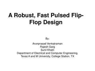
A Robust, Fast Pulsed Flip-Flop Design. By: Arunprasad Venkatraman Rajesh Garg Sunil Khatri Department of Electrical and Computer Engineering, Texas A and M University, College Station, TX. Introduction. High speed VLSI design uses heavy pipelining

E N D
A Robust, Fast Pulsed Flip-Flop Design By: Arunprasad Venkatraman Rajesh Garg Sunil Khatri Department of Electrical and Computer Engineering, Texas A and M University, College Station, TX
Introduction • High speed VLSI design uses heavy pipelining • Results in increased number of Flip-Flops • For mobile devices • Power consumption is the prime concern • Requires low power Flip-Flops • Also demand for high speed operation • Hence there is a strong need for Flip Flops with: • High speed • Low power • Low area • Tolerance to PVT variations
Figure of Merit - Timing • Time period T ≥ Tcq + Tsu + d • where d– delay of the combinational circuit • Tsu – setup time of the Flip-Flop • Tcq –clock to Q delay of the Flip-Flop • So Tcq + Tsu is the required figure of merit of the FF, since d is circuit-dependent
Traditional Flip-Flops • Data needs to arrive before the clock edge • So setup time Tsu is positive • Hence Tcq + Tsu is much higher • Want to design a flip-flop with a goal of minimizing the figure of merit Tcq + Tsu • We explored different circuit designs with this goal in mind, while ensuring that the resulting flip-flop achieves • Low power and area • High speed • Robustness to PVT variations
Pulsed Flip-Flops (P-FF) Latch Clk Data D Q Pulse Pulse Pulse Generator Clk Clk Data • Broadly: consists of a pulse generator + latch • Pulse is derived from clock edge • So pulse is generated after clock edge • Hence data can arrive even after the clock edge (therefore Tsu may be negative)
Proposed Pulsed Flip-Flop The proposed pulse generator design The latch structure
Operation of Pulse Generator Waveforms obtained at various nodes Clock falls, node Z is pulled up to VDD Clock rises, N2 discharges internal node W Until W discharges, N2 and N1 helps to discharge Z Very fast slew rates for falling edge of Z
Experimental Setup • Implemented our Pulse Flip-Flop in BPTM 100nm • Compared with other Flip-Flop designs • Explicit Flip-Flop • Improved hybrid pulsed Flip-Flop • Traditional D Flip-Flop • Performed Monte Carlo simulations for supply voltage (VDD), channel length (L), threshold voltage (VTH ) variations • 500 Monte Carlo simulations • 3σ = 10% for VDD, L and VTH
Pulsed Flip-Flops Compared Explicit Pulsed Flip-Flop Improved Hybrid latch Flip-Flop
Layout Comparison Proposed Pulsed Flip-Flop Master-Slave D Flip-Flop • Our proposed pulsed Flip-Flop has 27% lesser area than a traditional D Flip-Flop
Conclusions • We proposed a novel pulsed Flip-Flop (P-FF) design • The performance of our P-FF design is better than other FFs • 60% better Tcq + Tsu than other pulsed Flip-Flops • 40% lower power dissipation than explicit pulsed Flip-Flop • 27% lesser area than a master-slave D Flip-Flop • Our P-FF is more robust to process and voltage variations than other designs considered • Performed Monte Carlo simulations with varying VDD, L and VTH • Our design has the lowest standard deviation of Tcq + Tsu • We can further reduce area and power by sharing pulse generator circuit between several latches