Dislocations Dislocations Dislocations
Dislocations Dislocations Dislocations. Dislocations are very important imperfections in real materials. Dislocations are line imperfections in otherwise perfect lattices. Dislocations are formed during solidification, during processing or when the material is deformed.


Dislocations Dislocations Dislocations
E N D
Presentation Transcript
Dislocations Dislocations Dislocations • Dislocations are very important imperfections in real materials. • Dislocations are line imperfections in otherwise perfect lattices. • Dislocations are formed during solidification, during processing or when the material is deformed. • Dislocations strongly affect the mechanical, electronic and photonic properties of materials. • There are two basic types of dislocations – edge and screw.
The perfect crystal in a) is cut and sheared one atom spacing in b) and c). The line along which the shearing occurs is a screw dislocation. A Burgers vector b is required to close a loop of equal atom spacings around the screw dislocation.
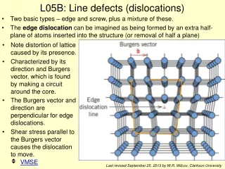
a) b) c) The perfect crystal in a) is cut and an extra plane of atoms is inserted in b). The bottom edge of the extra plane is an edge dislocation in c). A Burgers vector b is required to close a loop of equal atom spacings around the edge dislocation.
A mixed dislocation showing a screw dislocation at the front of the crystal gradually changing to an edge dislocation at the side of the crystal. Note that the line direction of the dislocation is parallel to the Burgers vector of the screw dislocation and perpendicular to the edge dislocation.
When a shear stress is applied to the dislocation in a) the atoms are displaced, causing the dislocation to move one Burgers vector in the slip direction b). Continued movement of the dislocation creates a step c) and the crystal is deformed. Motion of a caterpillar (or a fold in a rug) is analogous to the motion of a dislocation. Note: the slip direction is always in the direction of the Burgers vector of the dislocation.
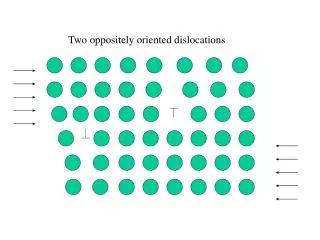
Stress at Dislocation Cores Stress contours around edge and screw dislocations. Edge dislocations are much more complex than screw dislocations. Stress field around screw dislocation. Stress field around edge dislocation.
The core of the dislocation can accommodate a small atom such as carbon more easily than the interstitial positions of the unit cell. The carbon increases the resistance of the dislocation to move by sliding on its habit plane. This is called Cottrell locking, which increases the strength of the steel and enables working hardening. Otherwise body centered cubic materials don’t work harden because they lack a close packed habit plane necessary for dislocation interactions by cross-slip.
Dislocations in Ti3Al seen by TEM showing dislocation pileups in a) and b) and how they contribution to permanent or plastic deformation in c).
Control of Dislocations • Control of dislocations allow us to manipulate mechanical properties and understand their temperature dependence. • When a shear force acting in the direction of the Burger’s vector is applied to a crystal containing a dislocation, the dislocation can move by breaking bonds between the atoms in one plane. • By this process, the dislocation moves through the crystal to produce a step on the exterior of the crystal. • The process by which the dislocation moves and causes a solid to deform is called slip.
Dislocation Slip • Dislocations move more readily in some crystal planes and directions than in others as we will see. • The slip direction of an edge dislocation is in the direction of the Burger’s vector. • A slip plane is defined by the direction of the Burger’s vector and the line direction of the dislocation • The line direction of a screw dislocation is in the same direction as its Burger’s vector. • An edge dislocation has its Burger’s vector perpendicular to the line direction of a dislocation • A dislocation having a line direction not parallel or perpendicular to the Burger’s vector is considered a mixed dislocation.
Dislocation Slip • During slip the dislocation moves from one set of surroundings to another identical set. • The least amount of energy expenditure requires movement in directions in which the repeat distance is shortest, i.e., close-packed directions. • Slip planes tend to be those planes with a high planar packing, i.e., close-packed planes. • Slip reduces strength but increase ductility in materials.
, u , b b b , R Schematic of slip line, slip plane and slip vector (Burgers vector) for a) an edge dislocation and b) a screw dislocation. Note the relationships between the dislocation line (u), slip vector (b) and glide plane (R) whereR = b x u.
u An edge dislocation in MgO. Dislocations in ceramics and semiconductors are complicated by charges existing at their core requiring large energies for them to glide. Fracture does not occur in these materials by dislocation glide but by cracks (surface defects). If these dislocations can’t glide, why do they exist and how do they move?
Defects in GaAs/InGaAs Laser Note that the laser looks to have a perfect crystal structure when using the 200[011] electron diffraction vector but actually has dislocations, which moved into the active region by creep, when viewed using the 220[110]. Dark lines are InGaAs layers and light lines are GaAs layers plus substrate and capping layers.
Dislocation Core Structure in GaAs Definition of alpha (Ga-core) and beta (As-core) dislocations: removal of the segment 1564 leads to the formation of an As-terminated dislocation and 1234 leads to the formation of a Ga-terminated dislocation. A Ga core will have excess holes whereas an As core will have excess electrons.
Dislocation-Dislocation Interactions A FCC material such as austenite can work harden because the dislocation can interact on the close packed planes, i.e., the {111}, having Burgers vectors in the close packed directions, i.e., <110>. Schematic of two dislocations interacting to form three dislocations.
Surface Defects • Surface defects are another type of imperfection in real materials. • They consist of the boundaries or planes that separate a material into regions of different crystal structure or orientation. • The material’s surface is one example • Grain boundaries are another example of a surface defect. • Others are stacking faults, twin boundaries and magnetic domain boundaries • As we saw in the electron images of the atoms (lattice images), grain boundaries are narrow zones where the atoms are not properly spaced in which tension or compression exists. • Grain size influences many material properties such as strength and electrical conductivity.
Grain boundaries showing in a) that the atoms at the boundaries near the three grains (referred to as a triple point) do not have an equilibrium spacing and in b) grains in a stainless steel sample.
b q/2 2D The angle, q, of a tilt boundary is made from three dislocations and can be described by the equation below. Note – Grain boundaries are a two-dimensional array of dislocations.
Low angle grain boundaries in Cubic Zirconia seen using by TEM Dickey et. al., Microscopy and Microanalysis (2000) pg. 120
Planar Defect – Stacking Fault A stacking fault is shown where atomic column “a” is interfaced with atomic column “b”, which resulted from the dislocations found on either end of the stacking fault.
Lattice Image of a "Stacking fault" in GaAs showing reverse ordering of Ga and As planes. Note the partial dislocation at the start of the fault. Kisielowski et. al. Microscopy and Microanalysis (2000) pg. 16
A twin boundary, which is a planar defect, is shown where a displacement of atoms by a stress reorients a volume of the crystal, which is bounded by the twin boundary.
The material Brass, a copper zinc alloy, deforms by the formation of twins. The twin boundaries are at the interface of the dark and line regions.
Formation of Twins Gradual reduction of twin width due to emission of dislocations from grain boundary original twin width Dislocation mechanism for twin boundary migration (reduction in width) using dislocations.
Twin boundaries and dislocations recently found in small LaF3 crystals. LaF3 is a light emitting diode material.
The End (Any questions or comments?)