Download
1 / 183
1.83k likes | 2.11k Vues
Explanation of band structure in linear chain of Fluorine atoms, orbital interactions, electron bonding, and energy calculations.

E N D
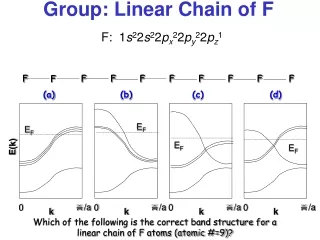
EF EF EF E(k) EF p/a p/a p/a p/a 0 0 0 0 k k k k Group: Linear Chain of F F: 1s22s22px22py22pz1 F F F F F F F F F F (a) (b) (c) (d) Which of the following is the correct band structure for a linear chain of F atoms (atomic #=9)?
There are 4 n=2 orbitals in the unit cell (a single F atom with 1 2s + 3 2p orbitals). Can you identify any of them? There is a lower 1s band (not shown) EF EF EF E(k) EF p/a p/a p/a p/a 0 0 0 0 k k k k Linear F Chain
Band Structure: Linear Chain of F Antibonding 2s s* Bonding 2s s A sigma bond shares only one electron Antibonding 2pzs* Bonding 2pz s Which one of these has lower energy? Will the other p orbitals look like this?
Band Structure: Linear Chain of F Antibonding 2s s* Bonding 2s s A sigma bond shares only one electron Antibonding 2pzs* Bonding 2pz s Which of these two p orbitals is doubly degenerate (which will we have two of)? A pi bond shares two electrons Antibonding 2px/2pyp* Bonding 2px/2pyp
EF EF EF E(k) EF p/a p/a p/a p/a 0 0 0 0 k k k k What do you think that limits our choices to? F F F F F F F F F F (a) (b) (c) (d) How do we determine between the final remaining?
Do the sigma and pi p orbitals have the same band width? What affects bandwidth? For the same lattice parameter, the reduced spatial overlap of the p interaction causes the p bands to be narrower than the s bands. Linear F Chain
Band Structure: Linear Chain of F Antibonding 2pzs* Doubly degenerate EF Antibonding 2px/2pyp* Doubly degenerate Antibonding 2s s* Bonding 2px/2pyp Bonding 2pz s Bonding 2s s 0 k p/a
Band Structure: Linear Chain of F A more accurate treatment of the band structure would show an avoided crossing between the 2pzs and 2s s * interactions at k=p/a. There would be mixing between these two bands (creating sp-hybrid like states). Antibonding 2pzs* EF Doubly degenerate Bonding 2px/2pyp Bonding 2s s 0 k p/a
The Need for Collaboration • No theoretical method perfectly describes real properties (will discuss some more soon) • Why? Not all physics is understood. Defects, strain, boundary effects, etc. can all have big effects! • Good models typically require a lot of computation time (weeks/months)! • The best models occur when experimentalists and theorists work back and forth to find a model that describes what is observed!
To understand rest of energy band calculations, helpful to understand a few concepts:One day on semiconductors(for more, take 772) After today’s class you should be able to: • Predict absorption in direct and indirect semiconductors • Understand what is meant by a quasiparticle • Calculate effective mass from simple energy bands
Many solids conduct electricity = n e2 / m ( = 1/) There are electrons that are not bound but are able to move through the crystal. Conducting solids fall into two main classes; metals and semiconductors. and increases by the addition of small amounts of impurities (semiconductors do opposite). In a metal, the conductivity (1/resistivity) normally gets smaller (or resistivity increases) at higher temperatures.Why? Why opposite?
A small fraction of electrons are thermally excited into the conduction band. These electrons carry current just as in metals. The smaller the gap the more electrons in the conduction band: fraction ~ exp(-Eg/2kBT) – show origin later Conductivity increases with temperature (more excited e-s) Semiconductors Simplified energy bands Semiconductor @ high Semiconductor @ low temp Insulator
Approximate the fraction of electrons in the conduction band at 300 K for semiconductors: Si (~1 eV), topological insulator Bi2Se3 (0.3 eV), and tin (0.1 eV). • The smaller the gap the more electrons in the conduction band: fraction ~ exp(-Eg/2kBT)
- Flat band structure in semiconductors The ground state is sometimes called the vacuum state Conduction band Forbidden band Electron energy Energy gap Valence Band = Dirac Sea of Electrons Eph>Eg If the incoming photon energy is higher than the energy gap, an electron can be excited
Optical Properties Flat band structure • If a semiconductor or insulator does not have many impurities or defects, photons with energies smaller than the band gap energy can’t be absorbed • What applications might this be useful for? • Sunglasses or Si filters (transmission of infra red light with simultaneous blocking of visible light) • This is why many insulatorsare transparent to visible light (e.g. glass), whereas semiconductors are not (qualifier ques)
Charge carriers (electrons or holes or both) created in the corresponding bands by absorbed light can also participate in current flow, and thus should increase the current for a given applied voltage, i.e., the conductivity increases This effect is called Photoconductivity If want conductivity to be controlled by light. Need what? Want few carriers in dark → gap not too small Want light to be absorbed, creating photoelectrons → Band gap of intrinsic photoconductors should be smaller than the energy of the photons that are absorbed Photoconductivity Solar spectrum
Direct gap semiconductors: the top of the valence band and the bottom of the conduction band occur at the same k-vector. Conduction band Energy Gap Valence band Gallium Arsenide GaAs Direct Gap Semiconductors L X
Direct gap semiconductor: sharp onset of absorption when the photon energy is equal to the bandgap Conduction Band Energy hn =Eg k Valence Band Bandgap of InSb at 4K is 0.23eV Direct Optical Absorption Optical absorption in the direct gap semiconductor InSb at 4K Photon creates an “electron-hole pair”
UV Visible Why does glass absorb IR but not visible? Onset due to band gap, which varies with type of glass Much of the infrared absorption of standard glass is due in part to residual –OH groups, which largely act like water in terms of their vibrational absorption spectra. “An ongoing challenge with these glasses is removal of impurities such as hydroxyl ions (OH−), which are characterized by absorption in the wavelength region of interest.” (http://spie.org/newsroom/3592-oxide-glasses-for-mid-infrared-lasers?SSO=1) Not a huge deal for your car, but think about laser systems!
What is a Greenhouse Effect? • During the day, the energy from the sun is absorbed by the things on Earth (us, plants, etc). • Just like your car interior, these things reemit the energy in the form of infrared radiation (what you see with night vision goggles) • The atmosphere acts a lot like your car windows, keeping the infrared (and therefore heat) on our planet. • Why it doesn’t get super cold at night, unlike the dark side of the moon (-280° F). Also why it doesn’t get super hot either (bright side of the moon is 260°F). • Greenhouse is good, but only if it doesn’t hold too much heat!
Indirect Gap Semiconductors Indirect gap semiconductors: the top of the valence band and the bottom of the conduction band occur at different k-vector. Direct bandgap 0.8eV Indirect bandgap @ k =0, is 0.66eV Germanium (Ge)
A transition across an indirect band gap requires a photon to be absorbed and a phonon (thermal excitation) to be absorbed or emitted. Conduction Band Energy kphonon hnphoton ~Eg k Valence Band Indirect Optical Absorption How would you expect the optical absorption to look this time?
Indirect gap semiconductor: no sharp onset of absorption 0.66 0.80 0.88 Ge: Indirect Optical Absorption 0.73 For T = 300K Eg (indirect gap) = 0.66 eV and EG1 (direct gap) = 0.8 eV How should this change with lower temperature? For T = 77K Eg (indirect gap) = 0.73 eV and EG1 (direct gap) = 0.88 eV Why bigger at low temp?
- What is a Quasiparticle? • Quasiparticles occur when a solid behaves as if it contained free particles. • Example: as an electron travels through a semiconductor, its scatters with electrons, phonons and nuclei; however it ~behaves like an electron with a different mass traveling unperturbed through free space. This "electron" with a m* is called an "electron quasiparticle". (m* =Effective mass) • Aggregate motion of electrons in the valence band of a semiconductor is the same as if the semiconductor contained positively charged quasiparticles called holes or positrons. Any others we have discussed? Conduction band Forbidden band Electron energy Energy gap Valence Band = Dirac Sea of Electrons
- Electron energy band structure in semiconductor Conduction band E Forbidden band Electron energy Energy gap + Valence band • Quasiparticles: excitations of the ground state (vacuum state), behave as if particles in free space • Excited electron leaves in the valence band a positive hole/positron. • Positive and negative charges are displaced in energy (not space), so…? • Positively charged hole interacts with negatively charged electron by Coulomb interaction.
Excitons (quasiparticle) are bound electron-hole states A free electron and a free hole (empty electronic state in the valence band)exert Coulomb force on each other: hydrogen-like bound states possible: excitonic states Eb is the excitonbinding energy = energy released uponexciton formation, or energy required forexciton breakup Note: exciton can move through crystal, i.e. not bound to specific atom!
Excitons in most semiconductors are not observable at room temperature, because of the low binding energy Quasiparticle in a box Light Hole and Heavy Hole bands (holes with different m*) On the other hand, excitonic emission is very important for opto-electronic applications, as it is narrow and highly energetic & can transport energy
Confused electron Confused hole Let’s focus on Effective Mass
EFFECTIVE MASS Real metals: electrons still behave like free particles, but with “renormalized” effective mass m* In potassium (a metal), assuming m* =1.25m gets the correct (measured) electronic heat capacity Physical intuition: m* > m, due to “cloud” of phonons and other excited electrons that slow it down (add mass) or speed up Interactions with the periodic crystal, electron-electron interactions and electron-phonon interactions renormalize the elementary excitation to an “electron-like quasiparticle” of mass m* Fermi Surface
Comparing free electrons and the electron quasiparticle Free electron Electron quasiparticle While electrons scatter, we treat electron quasiparticles like free electrons with m*. Thus, electron quasiparticles don’t scatter! (after their mass is renormalized)
Physical Meaning of the Band Effective Mass The effective mass is inversely proportional to the curvature of the energy band. Near the bottom of a nearly-free electron band m* is approximately constant, but it changes dramatically near the inflection point and even becomes negative(!) near the zone edge. What does that mean for electron near BZE?
Because the energy bands are different along different directions, the effective mass depends on which direction in k-space we are “looking” Effective Mass Which is heavier? Heavy and light holes have different bands so different effective masses (also different from electrons)
Conductivity in Semiconductors • What do we need to know in order to predict the conductivity for semiconductors. • For metals? • How did we find n, the density of conduction electrons, precisely for metals? = n e2 / m*
Electron and Hole Densities • To accurately determine the number of carriers in each band, we will modify what we derived for free electrons in metals • Electron Fermi-Dirac distribution function means what?
At a temperature T the probability that an available electron state is occupied is given by the Fermi-Dirac function If intrinsic, m is within the energy gap. In the conduction band Therefore Chemical potential or Fermi level • The chemical potential, m , is the energy for which f = ½ • (50% likely to be occupied). Fermi energy: all energy states are occupied below EF at T = 0 (metal). µ Then, how should f(E) change with temperature in a semiconductor?
Number of electrons in conduction band Silicon @ 300K n ~ 2x10¹⁶ m-3 log plot Note Units are cm-3 Electron density increases ~ exponentially with temperature (exponential would be straight line in log plot)
Electron and Hole Densities • To determine the number of carriers in each band, we will modify what we derived for free electrons • Fermi-Dirac distribution function for conduction (c) and valence (v) bands • What dependence on energy should the DOS have?
Assume: bottom of conduction band and the top of valence band parabolic conduction band E = Ec + 2k2/2me* valence band E = Ev - 2k2/2mh* Conduction band Valence band Conduction Band Valence Band D(E) E 0 Eg Density of States Conduction Band Ec = Eg Ev = 0 Valence Band 1
Electron density in conduction band Density of states Distribution function To find the electron density of occupied states:
Number of holes and electrons Exactly same argument for holes in the valence band gives Distribution function Total density of hole states Group: Find the product NeNh. As Ne=Nh(intrinsic) we can say: This result is important; known as law of mass action; find carrier density without µ. True for both intrinsic & extrinsic semiconductors.
Chemical Potential For intrinsic SCs, determine an approach that will find (the energy for which f = ½). When is = Eg/2? Results of recent discussion:
Silicon Eg=1.15eV m*e = 0.2me & m*h = 0.8me @ 300K. Gives Chemical potential near middle of gap Intrinsic semiconductors Ne=Nh In pure “intrinsic” semiconductors the electrons and holes arise only from excitation across the energy gap. Therefore Ne = Nh
Semiconductors can be easily doped Doping is the incorporation of impurities (different atoms) into a semiconductor in a controlled manner In a doped material, Ne is not equal to Nh Impurities change the electrical properties (e.g. conductivity) of the material, which can be useful for devices Doping Extrinsic Semiconductors
Impurties have a big effect on semiconductorsWhy? • Impurities add states within gap, excitation more likely • Impurities can get close enough to form their own bands • Causes the material to become a metal (Mott transition)
Let’s use Silicon (Si) as an example Substitute one Si (Group IV) atom with a Group V atom (e.g. As or P) Si atoms have four valence electrons that participate in covalent bonding When a Group V atom replaces a Si atom, it will use four of its electrons to form the covalent bonding What happens with the remaining electron? Donors
Donors • The remaining electron will not be very tightly bound, and can be easily ionized at T > 0K • Ionized electron is free to conduct • In terms of the band structure, this electron is now in the conduction band • Such Group V impurities are called Donors, since they “donate” electrons into the Conduction Band • Semiconductors doped by donors are called n-type semiconductors (extra electrons with negative charge)
This crystal has been doped with a pentavalent impurity. The free electrons in n type silicon support the flow of current.
Donors: Energy Levels • Such impurities create “shallow” levels - levels within the band gap, close to the conduction band • A donor is similar to a hydrogen atom (called hydrogenic donors) • A positive charge with a single electron within its potential • the small ionization energy means a sizable fraction of donor atoms will be ionized at room temperature
An electron added to an intrinsic semiconductor at T=0 would go into the lowest empty state i.e. at the bottom of the conduction band. When one adds a donor atom at T=0 the extra electron is bound to the positive charge on the donor atom. The electron bound to the positive ion is in an energy state ED = Eg- DE where DE is the binding energy. How much is E? -e ED +ve ion Ev = 0 Valence Band Another View: Hydrogenic Donors Conduction Band Ec = Eg DE
Treat Similar to Hydrogen • Employ the solution for hydrogen atom • Consider the energy of the bottom of the conduction band to be zero – “free” electron • Substitute the effective mass for the electron mass • Charge shielded in a solid so modify the Coulomb interaction by the dielectric constant of the solid (dielectric constant for free space, κ = 1)