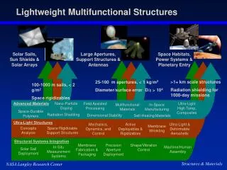
Spin Gain Through Multifunctional Oxide Electronics
Spin Gain Through Multifunctional Oxide Electronics. Novel Electronic Devices Based on Coupled Phase Transitions Workshop. Yuri Suzuki , University of California at Berkeley Oxide Materials and Heterostructures Andrew Kent , New York University Spin Current Devices

Spin Gain Through Multifunctional Oxide Electronics
E N D
Presentation Transcript
Spin Gain Through Multifunctional Oxide Electronics Novel Electronic Devices Based on Coupled Phase Transitions Workshop • Yuri Suzuki, University of California at Berkeley • Oxide Materials and Heterostructures • Andrew Kent, New York University • Spin Current Devices • Michael Flatté, University of Iowa • Device Theory
Abstract The growth of nearly atomically controlled complex oxide heterostructures has opened up a new class of materials with novel functionality, not observed in the constituent materials. We propose to develop a new class of tunable complex oxide devices with spin functionality, targeting the seamless integration of memory and logic, reconfigurable logic, and new sensing capabilities. Spin functionality may permit gateable control of an oxide device’s magnetization, spin transport/currents and/or spin wave propagation, including gated control of coupling between spin torque nano-oscillators (STNO)’s [1] as well as the demonstration and application of “spin gain”. Designing and generating spin functionality in quasi two dimensional electron gases (2DEG) systems, such as LaAlO3/SrTiO3 and LaTiO3/SrTiO3 heterostructures, is a promising route to multifunctional oxide electronics [2,3]. Spin functionality will be generated by doping the Mott insulator LaTiO3 with dilute amounts of 3d transition metal and 4f rare earth ions. The strength of the ferromagnetic coupling between magnetic ions embedded in these complex oxide heterostructures can be dramatically modified by tuning the electronic properties across their metal insulator transition, suggesting a new avenue for room-temperature gate-tuned control of ferromagnetism. If the oxide system were tuned close to, but not larger than the charge density needed for ferromagnetic transition, then a small spin current injected into the oxide heterostructure would push the electronic system over the edge towards the ferromagnetic state, and cause the resulting current moving through the oxide device to be highly spin polarized. This phenomena provides an essential and elusive device functionality, referred to as “spin gain”, which is currently missing from room-temperature spintronic device technology. As the strength of the spin gain will depend on the electronic density in the oxide material, these hybrid spintronic devices may allow electrical control of the spin gain, and thus controllable spin amplifiers. REFERENCES [1] F. Macia, A. D. Kent and F. Hoppenstead, “Spin-wave interference patterns created by spin-torque nano-oscillators for memory and computation” arXiv:1009.4116 and to appear in the Journal of Nanotechnology (2011). [2] F.J. Wong, R.V. Chopdekar, Y. Suzuki, “Disorder and Localization at the LaAlO3/SrTiO3 Heterointerface,” Physical Review B 82, 165413:1-5 (2010). [3] F. J. Wong, Seung-Hyub Baek, Rajesh V. Chopdekar, V.V. Mehta, Ho Wan Jang, C.B. Eom, and Yuri Suzuki, “Metallicity in LaTiO3 thin films induced by tetragonal lattice deformation,” Physical Review B RC 81, 161101 (2010).
Spin Gain Using Oxide Heterostructures Use magnetic oxides heterostructures to achieve new spin functionalities including spin-gain and high speed devices Spin as a state variable in electronics • Low power operation • Integration of logic, memory and sensors • Nonvolatile operation Spin gain needed for amplification and fanout • Present spin-device functionality based mainly on spin-filters Magnetic sensors (GMR, TMR) MRAM Spin-torque MRAM Spin-transistors
Spin Gain Using Oxide Heterostructures Exploit phase transitions in strongly correlated systems driven by currents and fields for new device functionality • Paramagnetic ⇔ Ferromagnetic • Nanostructured devices based on oxide heterostructures PM FM subthreshold swing of spin current << 60 mV/decade e.g. Nikonov+Bourianoff, IEEE Trans. Nano 4, 206 (2005)
Synthesis and Device Fabrication Nb-SrTiO3 substrate conducting AFM Atomic engineering of thin films and heterostructures Experience with LaTiO3/SrTiO3, LaAlO3/SrTiO3, CaMnO3/CaRuO3 and other heterostructures* Oxide junction heterostructures based on perovskites and spinels SrRuO3 SrTiO3 LaAlO3 SrRuO3 * Wong et al., PRB 81 161101(2010); Wong et al. PRB 82 165413 (2010); He et al. JAP to appear 2011 Vertical transport device structures Both conducting AFM measurements and patterned junctions (as in our previous magnetic tunnel junction studies) will be studied.† By careful choice of electrode material and thickness, we can maintain lattice distortions and hence metallicity in a LaTiO3 layer sandwiched between two electrodes †Hu et al., PRL 89 276601 (2002); Nelson-Cheeseman PRB 76 R220410 (2007); Nelson-Cheeseman PRB 81 214421 (2010).
High Speed Materials/Device Characterization • 100 ps rise / fall time, 5 V output amplitude (10 ps rise times in near future) • Recently added variable temperature capabilities • Characterization in frequency domain up to 50 GHz
Device Theory • Expertise in theory of: • spin transport in metals and semiconductors • magnetic ion interactions and phase transitions in dilute magnetic semiconductors • spin-orbit interactions in semiconductor quantum wells, including oxides • Example spin transistor device proposals
Room Temperature Ferromagnetic Oxide • Highly spin polarized La0.7Sr0.3MnO3 is a promising candidate for demonstration of spin manipulation via spin currents Surface spin polarization of LSMO Magnetic junctions based on LSMO We have shown that surface spin polarization of (110) LSMO recovers most readily as function of film thickness Junctions based on (110) LSMO electrodes exhibit distinct magnetic and resistive switching. Nelson-Cheeseman et al. PRB 76 R220410 (2007) Chopdekar et al. PRB 79 104417 (2009)
Designing “new” materials using correlated materials in proximity to a metal-insulator transition LaTiO3 is a bulk Mott insulator on the verge of a metal-insulator transition • Lattice distortions associated with epitaxial strain lead to metallic LaTiO3 films when the films are grown on SrTiO3substrates LaTiO3 films on different substrates Resistivity scaling of LaTiO3 films increasing compressive strain Films grown under little or no epitaxial mismatch with the substrate exhibit insulating behavior while those on SrTiO3 show metallic behavior Metallicity is primarily a bulk film effect NOT due to defects in the substrate, interdiffusion at the interface or charge transfer at the interface. Wong et al., PRB 81,161101(2010). 9 Novel Electronic Devices Based on Coupled Phase Transitions Workshop
Designing spin functionality LaTiO3 SrTiO3 LaTiO3 provides a platform for both 2D and 3D conductors into which we will design spin functionality Magnetic doping of the metallic gas via • B site doping of LaTiO3- 3d3 and 3d5 transition metal dopant ions such as Fe3+ and Cr3+ within LaTiO3 layer • A site doping of LaTiO3- 4f rare earth ions to induce FM • delta doping of FM layers- such as oxygen deficient LaMnO3 layers or uncompensated (111) surfaces of LaCrO3/LaFeO3 2D A B Ohtomo et al. Nature (2004) O ABO3 3D
AP – P Spin current devices Current pulse Spin current induced switching in nanostructures 50 x 50 nm2 ~10 electrons/spin • Switching speed is limited by conservation of angular momentum in transition metal nanostructures • Spin-current induced switching and instabilities will be explored in oxide heterostructure nanostructures D. Bedau et al., APL 96, 022514 (2010) & APL 97, 262502 (2010)
Current-induced magnetic instabilities SrRuO3 Tc = 150 K • Millisecond current pulses Feigenson, Reiner and Klein, Current-induced magnetic instability in SrRuO3, J. Appl. Phys. 103, 07E741 (2008). • Nanosecond current pulses
Summary • Targeting spin gain and functionality in oxide heterostructures • Spin current induced phase transitions • Spin current induced switching • Development of new oxide heterostructures with magnetic functionality • Fabrication of nanostructured devices • High frequency/speed device characterization • Device theory