Download
1 / 40
400 likes | 590 Vues
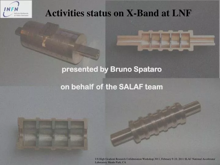
Activities status on X-Band at LNF. presented by Bruno Spataro on behalf of the SALAF team. US High Gradient Research Collaboration Workshop 2011, February 9-10, 2011 SLAC National Accelerator Laboratory Menlo Park, CA. Contributors. This work is made possible by the efforts :.

E N D
Activities status on X-Band at LNF presented by Bruno Spataro on behalf of the SALAF team US High Gradient Research Collaboration Workshop 2011, February 9-10, 2011 SLAC National Accelerator Laboratory Menlo Park, CA .
Contributors This work is made possible by the efforts : SALAF Group, INFN - LNF V. Dolgaschev,S. Tantawi , A.D. Yeremian, SLAC Y. Yigashi, KEK M . Migliorati, A. Mostacci, L. Palumbo, University of Roma 1 J. Rosenzweig et. al., UCLA R. Parodi,INFN-Genova M.G. Grimaldi et. al., Universityof Catania US High Gradient Research Collaboration Workshop 2011, February 9-10, 2011 SLAC National Accelerator Laboratory Menlo Park, CA
SUMMARY • Design and characterization of a p mode section at 11.424 GHz • Design and characterization of a p/2 mode section at 11.424 GHz • Technological activity status on electroforming, molybdenum sputtering, soft bonding and electro-beam welding. US High Gradient Research Collaboration Workshop 2011 February 9-10, 2011 SLAC National Accelerator Laboratory Menlo Park, CA
X-band structure Traveling Wave accelerating structures RF compressor RF GUN SALAF(LinearAccelerantingStructures at High Frequency) is the INFN r&d programm on “ multicell resonating structures” operating at X-band (10 ÷ 12 GHz). the MOTIVATION ……. To use in high brilliance photo-injectors (SPARC-phase-2) to compensate for the beam longitudinal phase-space distorsion, enhanced by the bunch compression of the acceleration process To gain know-how in vacuum microwave technologies Basic layout of the SPARC Linac US High Gradient Research Collaboration Workshop 2011 February 9-10, 2011 - SLAC National Accelerator Laboratory - Menlo Park, CA
Structure with no coupling tubes Structure with coupling tubes r = 10.477 mm (End Cell) r = 10.540 mm (Central Cells) r = 10.477 mm (End Cell) r1 = 1mm p = 13.121 mm h= 2 mm r2 = 4 mm p r2 h Study and simulation of a 9-cell SW π-mode X-band structure r = 10.54 mm p = 13.121 mm h = 2 mm r2 = 4 mm p h r2 p Symmetry planes r2/ = 0.15 US High Gradient Research Collaboration Workshop 2011 February 9-10, 2011 - SLAC National Accelerator Laboratory - Menlo Park, CA
100 80 60 40 20 Ez (MV/m) 0 -20 -40 -60 -80 -100 0 2 4 6 8 10 12 14 16 Z (cm) … simulation of 9-cell p-mode …. Ez With beam-tubes and constant cavity radius no flatness on-axis of the longitudinal E-field u With beam-tubes and reduced end-cells radius flatnesson-axis of the longitudinal E-field u
Frequency [MHz] Frequency [MHz] Mode [p] Mode [p] 11160.784 11152.818 1/9 0 11162.906 11183.868 2/9 1/8 11191.717 11219.481 1/4 1/3 11263.701 11235.333 3/8 4/9 11311.225 11287.522 1/2 5/9 11340.448 11356.593 2/3 5/8 11393.989 11386.000 7/9 3/4 11418.634 11416.834 7/8 8/9 11427.465 11427.704 1 1 … simulation of 9-cell p-mode …. structure with mirrors DISPERSION CURVE with and without beam-tubes ×106 structure with tubes K = 2.42 % h = 2 mm Coupling coefficient
Network Analyzer s11 DETECTION OF THE FUNDAMENTAL MODE RESONANCES BY THE INPUT COUPLER Transmission coefficient lateral probe-lateral probe INPUT COUPLER INDUCED MODES p-mode 11.424 GHz LONGITUDINAL INDUCED MODES 22 MHz p-mode 11.424 GHz Frequency (Hz) Frequency (Hz) Network Analyzer s21 Dispersion Curve Before-After Brazing US High Gradient Research Collaboration Workshop 2011 February 9-10, 2011 SLAC National Accelerator Laboratory Menlo Park, CA
NIM A 554 (2005) 1-12 π-mode Cu model RF measurements p-mode ACCELERATING ELECTRIC FIELD BEHAVIOR AFTER the 9-CELL TUNING FIELD FLATNESS ±1% Normalized longitudinal field profile E2/EM Length (arb. Units)
A p/2 biperiodic cavity: technical design Tuners p = 13.121 mm h = 2 mm r2 = 4 mm gap (coupling cell ) = 1 mm RF probe location The structure is designed for brazing Accelerating cell Axial Coupling cell A p/2 biperiodic cavity: 17 cells copper prototype NIM: A 586 (2008
p/2 Structure with closed stop-band rc.c. = 11.7218 mm r = 10.575 mm Simmetry planes Real structure with coupling tubes r = 10.557 mm (End Cell) r = 10.575 mm (Central Cells) r = 10.557 mm (End Cell) r1 = 1 mm 4 mm lc.c. = 1 mm P = 13.121 mm US High Gradient Research Collaboration Workshop 2011 February 9-10, 2011 - SLAC National Accelerator Laboratory - Menlo Park, CA t = 2 mm
dispersion curve withand without beam tubes p/2 11.6 The frequencies separation between the operating /2 frequency and the adjacent ones frequencies is about given by ΔF= 39MHz and ΔF= 36MHz against the operating mode bandwidth ΔF= 1.6 MHz. 11.5 11.4 Frequency (GHz) 11.3 11.2 From the spacing of the lower and upper cut-off frequencies, the coupling coefficient is given by K = 3.6%. Mode (rad) US High Gradient Research Collaboration Workshop 2011 February 9-10, 2011 - SLAC National Accelerator Laboratory - Menlo Park, CA
Copper prototype (p/2 mode) Field profile simulation vs measurements Field profile measurement Field Flatness ±2.5% p/2 z axis (cm) Dispersion curve Coupler feeding End cells antennas p/2
p-MODE COPPER PROTOTYPE MAIN PARAMETERS Average accel.field = 42 MV/m @ 3MW peak power In red, the theoretical values Peak surface electric field, Esur = 105 MV/m Power dissipation, Pd = 2.45 KW/m (assuming and duty cycle of 10-4 ) p/2-MODE COPPER PROTOTYPE MAIN PARAMETERS In red, the theoretical values Peak surface electric field, Esur (MV/m) = 102 Power dissipation, Pd = 2.68 KW/m (assuming a duty cycle of 10-4 ) US High Gradient Research Collaboration Workshop 2011 February 9-10, 2011 - SLAC National Accelerator Laboratory - Menlo Park, CA
X-band device realisation issue Guidelines: How to improve the high power performance (e.g. discharge rate) ? R&D on materials using materials with higher fusion temperature; avoiding the device heating at high temperature as done in conventional brazing R&D on fabrication techniques • Sintered Molybdenum (Bulk) R&D on material • Electroforming • Soft Bonding • Molybdenum sputtering on Copper • EBW (Electron Beam Welding) R&D on fabrication techniques
Copper and Molybdenum prototypes for the breakdown studies Photographs of the two X band cavities manufactured @ LNF Molybdenum brazed Cu brazed US High Gradient Research Collaboration Workshop 2011, February 9-10, 2011 SLAC National Accelerator Laboratory Menlo Park, CA
Tuning with the wall deformation Tool for deformation test ~1.6 MHz/mm3 Detail of the maximum deformation obtained inside the cell [Master thesis of M. Ronzoni – University La Sapienza – Rome] Frequency shift (MHz) Breakinglimit US High Gradient Research Collaboration Workshop 2011 February 9-10, 2011 SLAC National Accelerator Laboratory Menlo Park, CA
The reference case ... …….. 3-cell Copper – p mode - SW structure The model was designed to concentrate the RF field in the mid-cell to achieve high-gradient field, to investigate the discharge limits (V.A.Dolgaschev, SLAC) The COPPER model has been tested to SLAC for power testing. The Palladium-Copper-Silver (PALCUSIL) alloys were used with different composition (different melting points). Results of high-power test of the3-cell standing wave structure performed by … “V.A. Dolgashev, SLAC” 30 October 2008 US High Gradient Research Collaboration Workshop 2011 February 9-10, 2011 SLAC National Accelerator Laboratory Menlo Park, CA
US High Gradient Research Collaboration Workshop 2011 February 9-10, 2011 SLAC National Accelerator Laboratory Menlo Park, CA
3-cell Sintered Molybdenum Bulk p mode - SW structure The model was designed to concentrate the RF field in the mid-cell • Machining with the ‘tungsten carbide’ tools Q0 = 4800 (measured) Jim Lewandowski, SLAC, 1/14/09 • The PALCUSIL alloys were used for • brazingMolybdenum-Molybdenum and Molybdenum-Stainless Steel joints. ! Higher Power tests of the brazed model have been carried out at SLAC (V. Dolgashev et al.) Bad results
Sintered Molybdenum (bulk) issue long time for machining the cavity It is not easy to braze. It is likely to have a gas contamination and an uneven loading stress in the braze region (joints are not completely filled with alloy ). 300 nm roughness using ‘tungsten carbide’ tools
copper metal Electroforming R&D and Test B. Spataro, R&D on X-band Structures at LNF “ Electroforming” is a galvanotechnical process to fabricate a metal structure using electro-deposition of a metal (usually Copper) over a mandrel (usually Aluminum) in a plating bath of Cu-SO4 + H2SO4 (copper sulphate + sulphuric acid ) The Al-core is afterward chemically eliminated with NaOH (sodium hydroxide) treatment (for Al cores). Electroforming is a very attractive process, alternative to the brazing technology Mixed processes, like electroforming after cell manufacturing with standard techniques (Electroplating process), are under development, too. Electroforming properties : The speed of plating process is ≈ 0.6 mm/day Dimensional tolerances: ± 2.5 µm Surface finishing: 150 ÷ 200 nm (to be improved, studies are in progress); High device reproducibility. Basic scheme for the electroforming
…… Electroforming R&D and Test 5 cells mandrel of a Mo-Cu structure Aluminium mandrel of the RF coupler and cell ready for the electroforming Mo discs are already machined to be the iris of the electroformed cell Electroformed RF coupler and cell Another view of the coupler mandrel is shown US High Gradient Research Collaboration Workshop 2011 February 9-10, 2011 SLAC National Accelerator Laboratory Menlo Park, CA
…… Electroforming R&D and Test Fundamental mode response of Cu-Mo electroformed structure RF cells after removing the Aluminium core with alkaline solution (sodium hydroxide NaOH). Cross section of a Mo-Cu electroformed structure. Q0 = 5406 π mode The Mo discs with an external ribs improve the mechanical properties. Next step: to improve the quality of the Cu surface altered by the alkaline solution by depositing silver on the core or using other methods .…to be investigated !!! )
Electroforming: other materials Q0 = 5788 First Cu-ZrElectroformed model after baking US High Gradient Research Collaboration Workshop 2011 February 9-10, 2011 SLAC National Accelerator Laboratory Menlo Park, CA The color is due to Oxidation effect
From electroforming to elecroplating Cu encapsulated (electroplating) structure: measured -mode field profiles by bead-pull technique. Q0 = 7700 (measured) A 3 cell Cu OFHC structure, encapsulated by galvanoplastic procedure under vacuum leak test. Higher Power tests of the model have been carried out at SLAC (V. Dolgashev et al.) US High Gradient Research Collaboration Workshop 2011 February 9-10, 2011 SLAC National Accelerator Laboratory Menlo Park, CA
Schematic diagram of a DC magnetron plasma sourcee Sputtering activities ongoing at LNF ….. HUNZIGER COMPANY DEVICE Experimental set up for the RF Magnetron Sputtering Power 60 W Vacuum level 4*10-2mbar Deposition rate about 0.5 nm/sec
Sputtering activities ongoing at LNF ….. Aluminium dish treated with copper Two euro cents covered with aluminium A titanium-steel screw covered with copper film Aluminium cylinder covered with gold
Roughness behaviour of the Sputtered molybdenum on a Copper sample AFM (Atomic Force Microscopy) shows the surface of a copper sample before molybdenum sputtering AFM (Atomic Force Microscopy) image of deposited Molybdenum (100nm) on a copper sample by sputtering technique . The roughness of the film is comparable to that of the substrate. This indicates that the roughness is determined by the substrate.
Chemical composition as function of the Depth Profile of the 300nm molybdenum film on a copper with a thermal treatment [ measurements carried out by R. Parodi (INFN-Genova) Actually, measurement of the carbon concentration is affected by a strong error ( up to ~ 30% of the measured value) XPS (X ray Photoelectronic Spettroscopy) depth sensitivity is ~ 5-10 nm (depending by the analyzed materials). Mo Cu O2 C Results are in good agreement with RBS measurements carried out at the Catania University (G.M. Grimaldi et al.) except for the carbon (much less) The XPS (X ray Photoelectronic Spettroscopy) Depth Profiling technique using the PHI 5600Ci system is available at the unit of Genova of the INFN. The sputtering parameters are 1µA Argon Ion at 4Kev energy on a raster covering an area of 5x5mm centered on the monochromatic X Ray spot on the sample.
RBS (Rutherford backscattering spectrometry) spectrum (black line) and simulation (red line) obtained on Mo film 130 nm thickness deposited on a 2 μm SiO2 layer on top of a Si substrate (University of Catania). Mo film on a SiO2 layer roughness is in the range of 1- 2 nm The electrical measurement using the Van derPauw configuration, gives a resistivity of 10-3 Ω cm by about two orders of magnitude higher compared to a pure Mo film with a 100nm thickness, a difference compatible with the presence of oxides in the Mo. Mo and O surface scattering contributions are reported as green labels. The Mo film contains oxygen. The deposited film is characterized by a Mo concentration lower than a pure Mo film with a 100 nm thick (~20 % reduction with respect to a pure Mo film).
Micro-cracks investigations carried out with the Scanning Electron Microscope (SEM) on Copper dish machined at very low roughness (70 nm) sputtered with 600 nm of Molybdenum after a thermal treatment of 2 hours at 600 °C zoom Grain of powder The study of the sputtering approach as function of the deposited material depth , thermal treatment, chemical composition, morphological properties is in progress.
Some SEM RESULTS as fuction of the temperature and depth profile Fig. 2 : Copper dish machined at very low roughness sputtered with 300nm of Molybdenum after a thermal treatment of 2 hours at 600 °C. Fig. 1 : Micro crack on Copper dish machined at very low roughness sputtered with 600nm of Molybdenum after a thermal treatment of 2 hours at 600 °C. Fig. 4 : Copper dish machined at very low roughness sputtered with 300nm of Molybdenum after a thermal treatment of 2 hours at 300 °C. Fig. 3 : Copper dish machined at very low roughness sputtered with 600nm of Molybdenum after a thermal treatment of 2 hours at 300 °C.
Soft bonding 3 cells Cu prototype By brazing like at temperature a little less than 230°C ( Sn melting point) we obtain a good mechanical structure stability. Some tests with copper OFHC remade with different shapes among the contact surfaces gave good results in term of helium vacuum leak A Cu OFHC structure under vacuum leak test If contact surfaces are machined at a very low roughness (70nm), the thermal treatment after Sn deposition could be unnecessary. Vacuum tight very good has been obtained with a proper pressure applied to the structure with three bars Standard model should be realized with the soft bonding plus electroplating technique
Triple choke standing wave structure (A.D. Yeremian, V.A. Dolgashev, S.G. Tantawi, SLAC) http://accelconf.web.cern.ch/accelconf/IPAC10/papers/thpea065.pdf Preliminary 3D Model Studies on the mechanical drawings are in progress in order to separate vacuum and RF-joint to test molybdenum and hard alloy structures
Prototype ready to be used for the EB technique Use of the Electron Beam Welding technique EBW was used for a welding test of an X-band cavity sample. Cross section of the prototype 3 mm cavity Tool to keep together the 2 half-cavities during pre-bonding Sample pre-bonding @ 300°C EB welded sample The pre-bondingisused in ordertoprevent : 1) microgapsleftbywelding (on the cellsurface) [vacuum leakage tests gave about 10-10 mbar litre/sec 2) accidental pocket air inclusions 3) EBW damages in the internalsurfaceof the structure 0.04 mm 0.6 mm
…… use of the Electron Beam Welding technique Macrographic inspection of EB welded joints, made on a X-band test specimen The welding meets the requirements of the applicable specification SI 01.003 revA No cracks have been found in the fusion zone and in the heat affected zone. There are only small porosities at the root-side of the weld joint which are, however, within the limits of the specs. Moreover dimensional mechanical tests before and after welding gave negligible difference. pre-bonding zone The joints in the pre-bonding region demonstrated to work well and additional tests are in progress, too. EBW zone
Status of the R&D and future programs • Two X-band structures ( and /2 modes) have been characterized at low power RF; • One -mode 9-cells Cu section has been manufactured for higher power tests; • Hybrid photo-injector at 11.424 GHz (see J. Rosenzweigand A. Vallonitalks) • Technological activity : • a) R&D on sputtering method, soft bonding and new alloys with the SLAC, KEK, INFN/Genova, University of Cataniacollaboration; • b) Production of a 3-cell standard prototype (combination of the soft brazing-electroplating - molybdenum sputtering) with the SLAC-KEKcollaboration; • c) Electron Beam Welding (EBW) activity with the SLAC-KEKcollaboration; • d) Triple choke standing wave cavity realization with the EBW technique SLAC-KEK-LNF- University of Roma 1; • e) Power tests at SLAC (have been already carried out)in the frame of a M.O.U with INFN, on design, fabrication and test of X-band devices and high gradient power tests of innovative structures. US High Gradient Research Collaboration Workshop 2011 February 9-10, 2011 SLAC National Accelerator Laboratory Menlo Park, CA
Thank you very much for your attention !!! US High Gradient Research Collaboration Workshop 2011 February 9-10, 2011 SLAC National Accelerator Laboratory Menlo Park, CA