Download
1 / 25
250 likes | 407 Vues
Integrated Circuits and the Future of Semiconductors. MSE-630. The Electronics Industry is BIG Business!!. In 2008, global sales of semiconductor devices and components are projected to be $309 billion

E N D
Integrated Circuits and the Future of Semiconductors MSE-630
The Electronics Industry is BIG Business!! • In 2008, global sales of semiconductor devices and components are projected to be $309 billion • When incorporated into end-use components built on semiconductor devices, the market is projected to be 1.7 trillion dollars MSE-630
The Revenues of U.S.-based chip companies account for nearly half of global semiconductor sales and more than three-quarters of U.S.-owned chip manufacturing Capacity is located in the United States. The U.S. chip industry provides more than $100 mission annually to support research in U.S. Universities, invests $15 billion in R&D, and employs 226,000 people Technology exports account for 23% of total exports. 75% of the chip industry revenue is from export sales. MSE-630
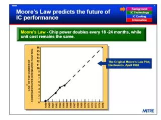
Historically, as the speed of devices increases, their size decreases The transistors manufactured today are 20 times faster and occupy less than 1% of the area of those built 20 years ago In a 1965 paper, Gordon Moore stated that the number of components on the most complex integrated circuit chip would double each year for the next ten years In 1965, there were 50-60 components on the average chip MSE-630
65nm Logic TechnologyIntel recently disclosed details of its 65 nm generation logic technology which includes numerous features to improve performance and reduce power. This technology is being demonstrated on fully functional 70 Mbit SRAM chips with over 1/2 billion transistors. Once again proving that Moore’s Law is alive and well, Intel’s 65 nm technology is on track for delivery in 2005. MSE-630
To continue to grow, the semiconductor industry has to overcome several technological challenges: • Lithography • Transistor scaling • Interconnections • Circuit families • Computer memory • Circuit design MSE-630
Moore pointed out in his original paper that the doubling 0f the number of components on an integrtated circuit was due to three factors: • Half the increase is derived from improvement in lithographic resolution • A quarter comes from larger chip sizes, made possible by improved manufacturing techniques and getter lithography • The remaining 25% is due to innovation, such as more creative techniques for forming components on a chip The industry will continue to grow so long as the rate of increase of components and functions on a chip exceeds the rate of increase of the cost per chip. MSE-630
Lithography Deep ultraviolet reduces dimensions to 250-nm. Smaller wavelengths present challenges due to diffraction of light and distortion, as well as photoresist materials Electron-beam lithography can, with l = 0.01-nm, has high resolution. Key problems include: -multiplicity of masks required -mask integrity -cost Historical and future trends of lithographic resolution capability Originally mercury lamps were used to get resolution of ~350 nm MSE-630
Lithography Proximity X-ray lithography has been used to fabricate ICs to 150-nm. The primary problem is that lenses and mirrors are not available for these wavelengths. Blocking masks must be used with features of the same dimension as that on the wafer. The cost and difficulty of fabricating thee masks without distortion are key challenges The biggest risk of any new lithographic technique is that the benefits derived from increased component density are outweighed by the increased cost. MSE-630
Transistor Scaling and Design The key tradeoff in technology adaptation is speed vs. cost. Bipolar transistors are faster than CMOS, but CMOS has higher circuit density – thus, CMOS wins out Comparison of projected vs. actual device performance For any reduction a in linear dimensions the voltage and doping levels can be adjusted to increase performance by a and decrease power density by a2 Trend of microprocessor clock frequency MSE-630
Transistor Scaling and Design Because devices operate at room temperature, off current limits designs to threshold voltages of 0.3V or higher Future improvements will require significantly lower operating temperatures Continued speed increases will require improved software and I/O design MSE-630
Shrinking components results in gate-oxide tunneling. The limit of a useful device with an on/0ff current ratio of 1000 due to source-drain tunneling alone appears to be about 5-nm separation between source and drain. Accounting for dopant fluctuations, the lower limit is likely 10-nm. • Possible advances in can come from: • Shorter channel lengths • Materials with higher performance Plausible evolution in transistor structure toward a more symmetric structure that results in better control of the fields in the gate region, regulating device condition. The FETs pictured are: (a) bulk Si, (b) silicon-0n-insulator (SOI), (c) ground plane, counter electrode (d) verticle double gate and (e) fully symmetric double gate MSE-630
Transistor Scaling and Design New device designs will move toward three-dimensional arrays of devices. These devices reduce space while using the same size components as current devices MSE-630
Low Temperature Operation • Operating at LN2 temperatures (77K) would improve performance by a factor of 2. Problems include: • Refrigerator cost • Reliability • Need to redesign technology to optimize low-temperature operation Optimum cost/performance operation may occur at -50oC using thermoelectric methods The best candidates for this are high-end servers MSE-630
Wiring and Connections Traditional interconnects are Al or Cu – both of which have resistance and capacitance Using materials with low dielectric constants in insulation layers allows continued decreases in size Another potential solution is to use a hierarchical wiring scheme, which combines high-density wiring at the first few levels with larger, lower-resistance and capacitance wires at upper levels MSE-630
Circuit Families Bipolar transistors generate more heat than CMOS Bipolar transistors win on speed – CMOS wins on device density Bipolar vs CMOS performance trends The large number of components on a chip lead to a superior system performance and lower cost per components. With more devices, more functions can be designed into a single chip. MSE-630
No alternative logic technology is evolving within cost/performance products on the market today to threaten CMOS dominance. In light of the continuing CMOS performance evolution, an even steeper evolution and learning curve would be required to displace CMOS. No radical shift in circuit type seems to be on the horizon. Moore’s law will continue to hold for approximately 10 more years MSE-630
Memory Cells The current limit in size is 4X the square of the lithographic dimension DRAM is a cell consisting of a transistor and capacitor. For the past 20 years, DRAM products have followed a generational evolution leading to a 4X increase in bits per chip every three years. In 1990, 1Mb of memory cost ~$175 retail. Now, a 1Gb DIMM costs $130 As lithographic improvements slow, so will growth of Memory MSE-630
Design The increase in function – the ways the devices on a chip can be arranged, will be the driving force for new ICs, not the sheer number of devices on a chip For a 10GHz processor, the clock cycle time is 100 ps. Since light travels at 300 mm/ps, in vacuum, the space reachable by light in one clock cycle is 30-mm. Assuming a medium consisting of typical dielectrics rather than vacuum, the reachable space is of the order of 15-20-mm, roughly the size of today’s chips. This places an upper bound on clock speeds and planar chip sizes MSE-630
Cost • Cost reduction is a major tenet of Moore’s law. The primary factor underlying the decreasing cost per circuit or memory bit is the increase in density, or circuits per square millimeter. The cost of processing a silicon wafer must increase much less rapidly than the density in order to achieve cost reduction. The rate of cost increase in the silicon chip manufacturing is approximately 15% per year. This si sdue to: • Stabilization of clean room requirements • Better equipment productivity and utilization • Slower increase in the number of process steps • The rate of increase in costs must be matched by a greater rate of increase of components per chip to continue to thrive MSE-630
Future Directions CMOS technology is likely to continue to evolve and dominate the semiconductor industry for the next 10-15 years • Optical lithography must be extended to unanticipated levels or be replaced by non-optical techniques. • Transistors must be replaced with a radical new structure • using new materials • DRAM cells must be designed in as-yet-unknown structures to achieve economically viable increase in memory chip integration • Wires must be fabricated at tenth-of-a-micron dimensions in hierarchical structure with low-dielectric constant materials • Dynamic circuits and SRAM cells must be designed to provide more function for a given set of transistors • Cost reductions will continue to be driven by the ability to integrate more functions on a chip MSE-630