Teaching Electronic Circuit Design: A Comprehensive Approach for Enhanced Student Engagement
110 likes | 227 Vues
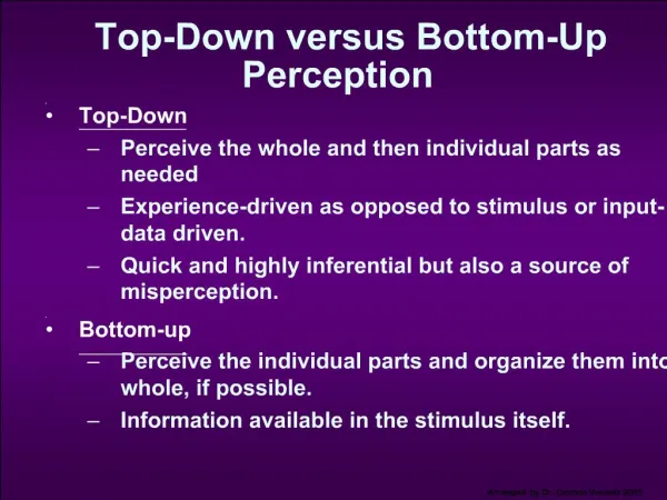
This course offers a dual approach to teaching electronic circuit theory and design by integrating both top-down and bottom-up methodologies. The curriculum covers essential topics such as operational amplifier block diagrams, biasing techniques, gain calculations, feedback stability, and the significance of trade-offs in design. Students are encouraged to adopt an application mindset while learning about bipolar and MOS transistor designs. The focus is on helping students grasp the interconnectedness of circuit elements and develop a strong foundational understanding of circuit optimization, enhancing their engagement and practical skills.

Teaching Electronic Circuit Design: A Comprehensive Approach for Enhanced Student Engagement
E N D
Presentation Transcript
Teaching Electronic Circuits Top-Down and Bottom-Up Tamara A. Papalias EE Dept – E365 San Jose State University San Jose, CA
Outline • Motivation • Op Amp Block Diagram • Bias Block • 2:1 Block • Gain Block • Output Buffer Block • Benefits • Summary
Motivation • Teach Students Circuit Theory • Analysis and Design • Teach Context of Structures • Teach Design Trade-offs • No “right” answer, just optimized • Encourage Application Mindset • Provide Roadmap for Sedra & Smith
Buffer A 2:1 Bias Bias Block Topics and Techniques Current Mirror Current Scaling Multiple Mirrors Transistor Sizing (BJT=area, MOS=W/L) Bandgap Topologies Simple Widlar Wilson Cascode Design Parameters Iout vs. Iin Output Resistance (Rout) Minimum Output Voltage (Vomin)
Buffer A 2:1 Bias 2:1 Block Topics and Techniques Differential pair ½ circuit model Active loads Clipping ADM vs. ACM Design Parameters Differential Gain (ADM) Common-Mode Rejection Ratio (CMRR) Bias Levels Output Swing/Headroom
Buffer A 2:1 Bias Gain Block Topics and Techniques Bode Plot Pole/Zero Identification & Analysis Miller Effect (Dominant Pole Approx.) Compensation Capacitor Negative Feedback Control Loop Shunt/Series Connections Design Parameters Gain Bandwidth Stability Gain Margin/Phase Margin
Buffer A 2:1 Bias Output Buffer Block Topics and Techniques Amplifier classes (A, B, C, D) Vout vs. Vin graph Crossover Distortion Clipping Short-Circuit Protection Effects of Loading (R & C) Design Parameters Linearity Efficiency (h) Slew Rate
Benefits • Bipolar and MOS can be taught side-by-side • Adds to discussion of trade-offs • Students begin to understand “good enough” • Students identify interaction b/tn blocks • Ex: How Rout of Bias sets CMRR with 2:1 block • Can assign design projects of complete or partial op amp for specific applications • Natural fit with SPICE commands • Students retain “big picture”
Feedback • Thank you • Any questions? • Personal note: • Students seem more engaged. • Some cultures have harder time adjusting to trade-off method instead of “exact answer”