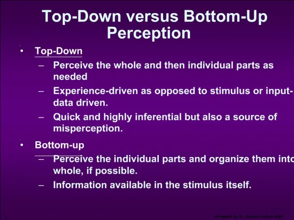
Top-down and Bottom-up Processes
Top-down and Bottom-up Processes. Presented by: Steven Price April 11, 2006. EE 518 Pennsylvania State University Instructor: Dr. J. Ruzyllo. Outline of Presentation. Top-down approach Bottom-up approach Why will it be needed? Applications Challenges of Bottom-up processing


Top-down and Bottom-up Processes
E N D
Presentation Transcript
Top-down and Bottom-up Processes Presented by: Steven Price April 11, 2006 EE 518 Pennsylvania State University Instructor: Dr. J. Ruzyllo
Outline of Presentation • Top-down approach • Bottom-up approach • Why will it be needed? • Applications • Challenges of Bottom-up processing • The future of top-down and bottom-up processing • Summary
Top-Down Approach • Uses the traditional methods to pattern a bulk wafer as in EE 418 lab. • Is limited by the resolution of lithography. http://pages.unibas.ch/phys-meso/Education/Projektstudien/Lithographie/Litho-M1-Lithography.html
What Constitutes a Top-down Process? • Adding a layer of material over the entire wafer and patterning that layer through photolithography. • Patterning bulk silicon by etching away certain areas. www.nanoscience.at/ aboutnano_en.html
Current Top-down Technology 193 nm ArF excimer laser photolithography stepper • Use of 193 excimer laser with phase shift masks to for features 65 nm in size. • Phase shift masks and complex optics are used to achieve this resolution. http://www.lrsm.upenn.edu/~frenchrh/lithography.htm
Problems with the Top-down Process • Cost of new machines and clean room environments grows exponentially with newer technologies. • Physical limits of photolithography are becoming a problem. • With smaller geometries and conventional materials, heat dissipation is a problem. http://www.cit.gu.edu.au/~s55086/qucomp/gifs/intro.moore1.gif
Bottom-Up Approach • The opposite of the top-down approach. • Instead of taking material away to make structures, the bottom-up approach selectively adds atoms to create structures. http://idol.union.edu/~malekis/ESC24/KoskywebModules/sa_topd.htm
The Ideas Behind the Bottom-up Approach • Nature uses the bottom up approach. • Cells • Crystals • Humans • Chemistry and biology can help to assemble and control growth. http://www.csacs.mcgill.ca/selfassembly.htm
Top-down Versus Bottom-up Top Down Process Bottom Up Process Start with bulk wafer Start with bulk wafer Alter area of wafer where structure is to be created by adding polymer or seed crystals or other techniques. Apply layer of photoresist Expose wafer with UV light through mask and etch wafer Grow or assemble the structure on the area determined by the seed crystals or polymer. (self assembly) Etched wafer with desired pattern Similar results can be obtained through bottom-up and top-down processes
Why is Bottom-Up Processing Needed? • Allows smaller geometries than photolithography. • Certain structures such as Carbon Nanotubes and Si nanowires are grown through a bottom-up process. • New technologies such as organic semiconductors employ bottom-up processes to pattern them. • Can make formation of films and structures much easier. • Is more economical than top-down in that it does not waste material to etching.
Self Assembly • The principle behind bottom-up processing. • Self assembly is the coordinated action of independent entities to produce larger, ordered structures or achieve a desired shape. • Found in nature. • Start on the atomic scale.
Applications of Bottom-Up Processing • Self-organizing deposition of silicon nanodots. • Formation of Nanowires. • Nanotube transistor. • Self-assembled monolayers. • Carbon nanotube interconnects. http://web.ics.purdue.edu/~mmaschma/bias_image_gallery1.htm
Self-organizing Deposition of Silicon Nanodots. • Most common applications are in optical devices and memory. • Silicon nanodots are deposited onto silicon dioxide with no need for lithographic patterning. http://www.iht.rwth-aachen.de/en/Forschung/nano/bottomup/deposition.php
Making Nanodots Process for making nanodots • Apply layer of self-assembled polymer film. • Grow layer of desired material to create nanodot. Polymer template for nanodot 65 billion nanodots per square cm http://news.bbc.co.uk/1/hi/sci/tech/33010241.stm
Nanodots Each nanodot can hold one bit of information. 13 nm high 80 nm wide 10 Trillion dots per square inch. Self Assembled Nanodots http://physics.nist.gov/Divisions/Div841/Gp3/Projects/Atom/atom_dots_proj.html
Properties of Carbon Nanotubes • Stronger than steel • Multiple tubes slide inside of each other with minimal effects of friction. • Electrical current density 1000 times greater than silver or copper. • Can range from having metallic properties to semiconductor properties based on it’s configuration. http://en.wikipedia.org/wiki/Nanotubes
Types of Carbon Nanotubes Semimetallic and semiconducting metallic http://www.tipmagazine.com/tip/INPHFA/vol-10/iss-1/p24.html
Growing Carbon Nanotubes • Deposit few particles of Iron (most common) to act as catalyst. • Apply a hot environment of carbon containing gas (typically CH4) • The particle catalyzes the decomposition of the gas and carbon dissolves in the particle. • When the particle is supersaturated with carbon, it extrudes the excess carbon in the form of a tube. http://www.phys.hawaii.edu/~sattler/Archives/archives91-94Apr7-2.htm
Nanotube Transistor • Basic diagram for a nanotube transistor • Benefits of transistor over conventional designs: • Smaller • Faster • Less material used • Many of the problems associated with conventional devices are solved www.nanotech-now.com/ news.cgi?story_id=06788
Nanotube Transistor-self Assembled Amine silane Ti/Au Contact AFM Image SiO2 Carbon Nanotube Diagram of Nanotube transistor www-drecam.cea.fr/.../ LEMautoassemblage.html
Nanotube Transistor Construction by DNA • DNA strands connect to gold electrodes on top of silicon. • DNA strands connect to ends of carbon nanotube. • Silicon and nanotubes are mixed and the DNA makes the connections to form nanotube transistors. http://www.trnmag.com/Photos/2004/121504/DNA%20makes%20nanotube%20transistors%20Image.html
Problem With Carbon Nanotube Transistors • Interface between metal electrodes and carbon nanotube is very sensitive. • Changing just one atom can significantly affect transistor performance. • Self-assembling nanotubes is not efficient. • Growing nanotubes in place has had little success. http://www.thomas-swan.co.uk/pages/nano_images.html
Self-assembled Monolayers (SAMS) • Molecules are deposited molecule-by-molecule to form a self-assembled monolayer. • Creates a high quality layer of material. • Layers are deposited one layer at a time. http://www.mtl.kyoto-u.ac.jp/english/laboratory/nanoscopic/nanoscopic.htm
Monolayers • Organic molecules can’t be deposited using extreme conditions because it would damage the organic molecules. • SAMS technique does not damage organic molecules. • SAMS films are nearly defect free. • Used to deposit organic semiconductors. http://www.orfid.com/images/img-vofet1.gif
Carbon Nanowire Interconnects • Metal contact acts as a catalyst to promote one-dimensional crystal growth. • Can one day be implemented as interconnects. Silicon Nanowire Diameter <1nm http://www.iht.rwth-aachen.de/en/Forschung/nano/bottomup/nanowires.php
Nanotube Interconnect Process http://www.nasa.gov/centers/ames/research/technology-onepagers/carbon_nanotubes_vertical.html
Benefits and Challenges of Nanotube Interconnects • Can have a much greater conductivity than copper. • Is more heat resistant than copper. • Carries a much larger current than copper. • Orientation of carbon nanotubes remains a problem. • Technology is not reliable enough to be used in device manufacturing. Carbon nanotubes grown on a metal contact through PECVD. Carbon nanotubes after layer of silicon dioxide added. http://www.nasa.gov/centers/ames/research/technology-onepagers/carbon_nanotubes_vertical.html
Challenges for the Bottom-Up Approach • Making sure that the structures grow and assemble in the correct way. • Forming complex patterns and structures using self assembly. • Contamination has a significant impact on devices with such small geometries. • Fabricating robust structures.
Strategies for Bottom-Up Processing • Combination of top-down and bottom-up processes to simplify construction. • Use catalysts and stresses to achieve more one-directional growth. http://www.isnm2005.org/_metacanvas/attach_handler.uhtml?attach_id=296&content_type=application/pdf&filename=Paper%2036.pdf
Future of Top-down and Bottom-Up Processing http://www.imec.be/wwwinter/business/nanotechnology.pdf
Advancements Made so Far • Carbon nanotube transistor (Stanford U.) • Organic monolayers for organic transistor (Yale U.) • Nanotube based circuit constructed (IBM) • Nanomotors and gears created (NASA) http://snf.stanford.edu/Education/Nanotechnology.SNF.ppt
What to Look For Nanotube array possibly used in future televisions. • Vias and interconnects being implemented with carbon nanotubes. • Nanotube transistors replacing conventional designs. • SAMS being used to create organic semiconductor based devices. • Carbon nanotubes becoming more and more prevalent as their growth is controlled. http://www.engin.brown.edu/Faculty/Xu/
Conclusion • Top-down processing has been and will be the dominant process in semiconductor manufacturing. • Newer technologies such as nanotubes and organic semiconductors will require a bottom-up approach for processing. • Self-assembly eliminates the need for photolithography. • Bottom-up processing will become more and more prevalent in semiconductor manufacturing.