DRAM
DRAM. Bob Reese Micro II ECE, MSU. SRAM - Static RAM. Fast ( cycle time = access time < 10 ns) In PCs, used for motherboard cache Basic cell is 6 transistors Expensive per bit. DRAM - Dynamic RAM. Basic Cell is one transistor + 1 capacitor

DRAM
E N D
Presentation Transcript
DRAM Bob Reese Micro II ECE, MSU
SRAM - Static RAM • Fast ( cycle time = access time < 10 ns) • In PCs, used for motherboard cache • Basic cell is 6 transistors • Expensive per bit
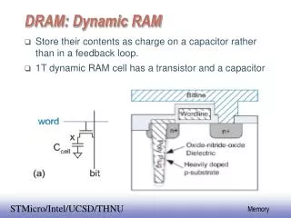
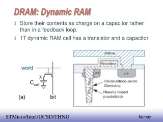
DRAM - Dynamic RAM • Basic Cell is one transistor + 1 capacitor • contents will leak off if not accessed periodically • Dense, cheap per bit • In PC’s used for main memory
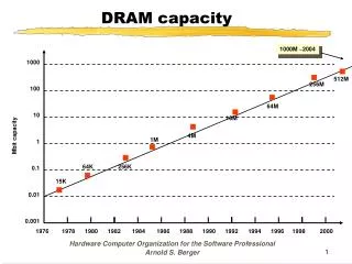
DRAM Architecture • Address bus is multiplexed between ROW and COLUMN address • 16 Mb would normally need 24 address lines, uses 12 address pins on DRAM • Row Address Strobe (RAS), Column Address Strobe (CAS) used to latch addresses. • Each new DRAM generation adds another address pin => double the total bits of previous generation 1975 1979 1982 1985 1988 1991 1994 1997 2000 4Kx1 16Kx1 64Kx1 256Kx1 1Mx1 4Mx1 16Mx1 64Mx1 256Mx1
Read Mode Comments • Access time is NOT EQUAL to cycle time • Need a recovery time (used for precharge of column bit lines) after a memory cycle if next cycle is to a different row. • Tcyc = Tras + Trp = 95 ns • If subsequent accesses are within the same row, then can use a fast page mode • Does not require recovery time • cycle time = 35 ns • DRAM control logic has to detect if next address is to same row or not and use the appropriate timing.
EDO DRAM • EDO => Extended Data Out • This is a version of page mode in which the output drivers are turned off at the falling edge of the CAS for the next cycle instead of the rising edge of the current cycle. • Data is available for longer, allows for tighter timing. • Improvement is on order of 10% - 15% • May not seem like much, but in hyper-competitive DRAM market, any edge can mean big dollars.
DRAM Refresh • A cell will loose its contents if not accessed periodically • Asserting the row select will refresh all cells in that row. • IBM 16M DRAM has 4096 rows, requires 4096 cycles. Refresh rate is 64 ms for 5V part, 256 ms for 3.3V part • Row address be externally provided or generated from an internal counter (the refresh counter in hidden refresh or self refresh modes)
Some DRAMs support a self refresh mode. One use is in low power DRAMs where DRAM refreshes itself during sleep mode so the DRAM controller can be sleeping as well to conserve power.
Speeding up DRAMs • Even a fast page mode cycle time of 35 ns (~ 30Mhz) is slow compared to SRAMs (< 10ns) • Latest DRAM innovation is the SDRAM - Synchronous DRAM • Adds a clock to the interface - all signals latched on clock edge • Optimized for burst transfers - supply an address, then succeeding clock cycles access sequential bits • IBM 16M SDRAM has clock speeds of 83, 100 Mhz!!! • All motherboards will use SDRAMs by next year.
Burst Transfer Optimization • Why should burst transfers be optimized for DRAMs? • CPU random accesses all go to the cache (SRAM) • If the data is not in the cache, the cache controller will transfer the needed block of data from DRAM to the cache, and write the old block back to the DRAM. • Block sizes vary, usually 32 to 256 bytes • DRAM is never accessed randomly - all reads/writes are block reads/writes.
IBM 4Mx4 SDRAM
Advantages of 2 banks • SDRAM has two internal memory arranged in two banks. • Row accesses can be ‘interleaved’ between the two banks such that while a row in bank 0 is being accessed, bank 1 is being precharged. • In many cases, can eliminate the precharge penalty for accessing two different rows!!!
Other SDRAM Features • In addition to the clock pin, added a new pin called CS (command select) • When asserted, the RAS, CAS, WE, and address pins are used collectively as a COMMAND. • The command specifies one of the many new transfer methods for the SDRAM • Also used to load the new internal mode register.
For burst mode, address only provided for first data, internal counter provides subsequent addresses.
DRAM Packaging • Need to get as much DRAM as possible into as small as space as possible on PC motherboards • SIMM (single inline memory module) and DIMM (dual inline memory module) are small circuit boards with multiple DRAM chips • SIMM gives a 32-bit memory path, DIMM a 64-bit memory path (needed when 64-bit CPU busses became common, eg. the Pentium!). • Current largest available DIMM is a 128MB
The Future: SLDRAM? • Facts: • DRAM is going to get denser, CPUs faster, even SDRAMs will not be able to keep up with CPU speeds. • SLDRAM => SyncLinkDRAM • Differential signaling on data, command pins • aiming for 400 Mb/s pin rates in burst mode • Still in planning stages, backed by consortium of major semiconductor memory players.