Download
1 / 23
230 likes | 260 Vues
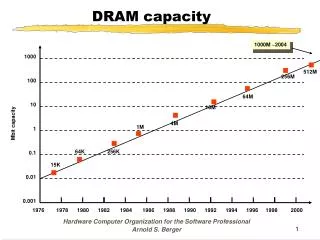
Direct Rambus DRAM (aka SyncLink DRAM). Goal High Density, Low Cost, High Bandwith DRAM To achieve high bandwidth to memory interface can either: make interface to memory faster make interface to memory wider Wider => More Chips or More Pins => More Cost

E N D
Direct Rambus DRAM (aka SyncLink DRAM) • Goal • High Density, Low Cost, High Bandwith DRAM • To achieve high bandwidth to memory interface can either: • make interface to memory faster • make interface to memory wider • Wider => More Chips or More Pins => More Cost • e.g., “wider is NOT necessarily better” • more chips also decreases reliability
Speeding up the interface • Many benefits to speeding up the interface instead of widening the datapath • Fewer pins, fewer chips => less cost • higher reliability • Rambus DRAMS or SyncLink DRAMs uses 400 Mhz bus based on Gunning Transceiver Logic (GTL) • Basically same approach as used with Pentium II local bus
Pentium II GTL Bus (Host Bus) • Gunning Transceiver Logic (GTL) used for Pentium II local bus (66Mhz now, 100Mhz later) • GTL bus is open drain bus where all runs are terminated • Termination voltage (Vtt) is 1.5 v. • GTL bus is a differential bus with only wire! • Vref used by all receivers, drivers • Vref (1.0v) is 2/3 of Vtt . • Voltage swing about Vref is +/- 200 mv. • Less voltage swing => higher speed, less noise margin
GTL Bus (continued) • Interconnections on a GTL bus are transmission lines so interconnect topology, termination very important. • Interconnection is point to point to avoid stubs (stubs generate reflections)
RDIMM RDIMM RDIMM Signaling Technology for RDRAM basically the same as PentiumII bus. RDIMMs must be connected serially to avoid stubs. Termination Resistors
SDRAM DIMM SDRAM DIMM SDRAM DIMM Normal Bus Topology for DRAM SIMMs.
IEEE Micro Nov/Dec 1997 18 bit wide external data bus which expands into 128 bit wide datapath internal to chip
Bandwidth • External bus is 18 bits wide (2 bytes + 2 parity bits) • External clock cycle is 400 Mhz, but data is clocked on each edge • Actually, external clock is a differential pair and data is sampled at each crossing • Total Bandwidth is 1.6 GBytes/s • 2 bytes * 400 Mhz * 2 edges => 1.6 Gbytes • Initial configurations are 4 M x 18 (72 Mbits)
Comparison • Recall that the Voodoo2 board had a 2.2 GB/s memory interface, used fast EDO DRAM • 12MB total, took 24 chips (two rows of 12, interleaved, used 256K x 16) • Would only need two RDRAM chips • 16 MBytes total (actually more than this, each byte is ‘9’ bits). • Data Rate => 3.2 GB/s • Drawback is that we would need two separate RDRAM controllers, one for each chip if we want to double bandwidth. • Some new Digital Signal Processors (DSP) already support the RDRAM interface
Uneven Net Loading in Conventional DRAM IEEE Micro Nov/Dec 1997
IEEE Micro Nov/Dec 1997 Loading increases linearly as # of RDRAM chips increase. Makes for easier timing design.
Internal Architecture IEEE Micro Nov/Dec 1997
Portion of internal architecture ( 4M x 16 or 4M x 18) 16 banks of 512 rows of 64 dualocts (1 dualoct = 16 bytes = 128 bits) 24 (banks) * 29 (rows) * 26 (dualocts) * 27 (one dualoct) = 226 (64 Mbit) A dualoct is the smallest addressable unit.
Addressing • 3-Bit Row bus used to give commands to RDRAM • ROW Activate command used for read • 4 clocks transfers 8 groups of 3 bits over Row bus due to dual edge clocking (24 bits total) • 24 bits in Row Activate command split between device address (6 bits), bank select (4 bits), row select (9 bits), and reserved bits • There are no chip select lines, internal register holds device address • All chips monitor bus - if bus device address matches internal id, then chip is selected.
Row Activate Command 10 ns R bits = row select DR bits = device address BR bits = bank select
Deep Pipelining => High Latency IEEE Micro Nov/Dec 1997 16 bytes transferred because 4 clocks * 2 edges * 2 bytes/transfer (external bus is 16 or 18 bits wide). 20 clock latency
Maximum Bandwidth • Note that maximum bandwidth with one RDRAM controller is 1.6GB/s. • Only one RDRAM chip can be active at a time on RDRAM bus. • More RDRAM chips increase capacity, not bandwidth. • With normal DRAM and SDRAM, can increase bandwidth by just adding more DRAM chips in parallel from same DRAM controller • To double the bandwidth, would need two separate RDRAM controllers
RDRAM Controller 100 MHz Local Bus 400 MHz RDRAM Bus
Nintendo 64 4 major chips: MIPS RS4300i CPU Reality Engine (Graphics) Two RDRAMs Memory bandwidth of 562MB/s, 31 pin interface to Memory controller. Memory took small amount of board estate, pin count. Used first generation RDRAMs.
The Future of RDRAM • Intel’s 1999 PC Motherboard spec has RDRAM as the base DRAM technology. • 100 Mhz SDRAM will only last through 1998. • Using multiple RDRAM channels, can get extremely high data bandwidths • Bandwidth = N * 1.6 GB/s where N is the number of channels
PC99 • PC99 Spec is Intel/Microsoft Spec for 1999 PCs • Five specs: Consumer, Office, Entertainment,Mobile, Workstation • For Graphics Adapters, Accelerated 3D graphics is REQUIRED • Must support both OpenGL and Direct3D • Support 800x600x16bpp, double-buffered, with Z-buffer. • Required support for multiple texturing on Entertainment PC (at least two textures in one pass) • More than one texture mapped to same object • Requires TWO sets of Texture coordinates.
Other Required Graphics Features • Flat and Gouraud Shading • MIP-mapped textures • Bilinear or better filtered textures, with perspective correction • Specular Highlighting • Alpha Blending • Depth-based fog (one Fog color) • Per-Vertex Fog (different fog color for each vertex)
Recommendations • Support maximum texture size of 2048 x 2048 • Support texture map sizes that are not a power of two • Texture unit can then be used to emulate BitBlt • Range-based and Table-based fog • Sort-independent edge anti-aliasing • Setup for Triangle strips and Triangle fans • Multi-Texturing Support