Advanced Data Processing in ALICE: FEE & GTU Development Insights
790 likes | 920 Vues
This document details the architectural and technological innovations in Fast Data Processing for the ALICE experiment at CERN. It covers key aspects such as FEE partitioning, design considerations for testing, optical readout systems, and global tracking units. The paper highlights the challenges in managing over 1.2 million channels and achieving high peak data rates of 16 TB/s. Emphasis is placed on the design flow of digital chips, the importance of low latency, power efficiency, and reliability in FEE development. Insights on chip design, detector simulations, and trigger functionalities are also provided.

Advanced Data Processing in ALICE: FEE & GTU Development Insights
E N D
Presentation Transcript
Fast Data Processing in ALICE TRD FEE & GTU • Introduction • FEE partitioning • Design for Test • Optical Readout • Global Tracking Unit Venelin Angelov Kirchhoff Institute of PhysicsChair of Computer Science Prof. Dr. Volker Lindenstruth University Heidelberg, Germany Phone: +49 6221 54 9812 Fax: +49 6221 54 9809 Email: angelov@kip.uni-heidelberg.de WWW: www.ti.uni-hd.de
TRD Structure stack MCM 6 planes 18 channels module max. 16 padrows 8 MCM 144 channels r z PASA • 1.2 million channels • 1.4 million ADCs • peak data rate: 16 TB/s • ~65000 MCMs • processing time: 6 µs TRAP TR-detector ORI ORI B=0.4T vertex 5 module rings 1080 optical links @2.5Gbps G T U 18 Supermodules in azimuth
Line Fit & Global Tracking module profile track virtual plane projected tracklets tracklets tracklet processor • straight line fit via a linear regression method • searching for dedicated patterns (for energy cut and electron - pion separation) • raw data buffer global tracking • projection of ‘tracklets’ to a virtual plane • searching for tracklets belonging together • perform (accurate) energy cut and generate trigger
FEE development • Howto design the FEE with so many channels? • - fast and with low latency • low power - precise power control (1mW/channel → 1.2kW) • low cost • minimize using connectors • use some simple chip package (MCM + ball grid array) • standard components? which process? IP cores? • flexible, as much as possible • make everything configurable • use CPU core(s) for final processing • reliable, no possibility to repair anything later • redundancy, error and failure protection • self diagnostic features
FEE development(2) Chip Design flow Detector simulations to understand the signals we get and what kind of processing we need Select PASA shaping time, ADC sampling rate and resolution Behavior model of the digital processing including the bit-precision in every arithmetic operation Estimate the processing time and select the clock speed of the design (multiple of LHC and ADC sampling clock) Code the digital design, simulate it, synthesize it, estimate the timing and area, optimize again… Submit the chip, this is the point of no return! Continue with the simulations, find some bugs and think about fixes Prepare the test setup And so on, TRAP1, 2, TRAPADC, miniQPM, TRAP3, TRAP3a (final)
Partitioning, Data Flow & Reduction MCM - Multi Chip Module L1 trigger to CTP TRD PASA ADC Tracklet Preprocessor TPP Tracklet Processor TP Network Interface NI GTU to HLT & DAQ event buffer store raw data until L1A detector 6 layers 1.2 million analog channels charge sensitive preamplifier shaper 10 Bit ADC 10 MSPS 21 channels digital filter preprocess data event buffer fit tracklets for trigger functionality process raw data monitoring builds readout tree for trigger & raw data merge tracklets into tracks for trigger process raw data for HLT time: data / event: peak rate: mean rate: reduction: during first 2 µs (drift time) 33 MB 16 TB/s 257 GB/s 1 after 3.5 µs after 4.1 µs max. 80 KB 600 GB/s - ~ 400 after 6 µs some bytes - - to trigger decision
Detector Readout 0 1,200,000 channels, 1,400,000 ADCs 10 bit 10 MSPS, 20 samples/event preprocessing Pretrigger MCM A + D 3+own:1 Drift 2 65,000 MCMs, 18+3 channels/MCM, 4 CPUs at 120 MHz 4:1 BM 4:1 HCM Merger 4 Processing 4,100 Readout Boards, 16+1(+1) MCMs 8 bit 120MHz DDR readout tree ORI 12 optical links . . . Transmission time 5:1 TMU 1,080 Optical Readout Interface links 2 links/chamber at 2.5 Gb/s G T U SMU x18 4.6 . . . 90 Track Matching Units (GTU) 1 TMU/module, FPGA based DDL TGU GTU 6 finished Central Trigger Processor CTP time [µs]
TRAP development – a long long way TRAP1 UMC 0.18μm FaRo1 AMS 0.35μm PASA AMS 0.35μm MCM for 8 channels with the first prototypes of the Digital chip and Preamplifier, commercial ADCs Beg 2001 First tested TRAP chip, in „spider“ mode Summer of 2002
Multi Chip Module 4 cm PASA Internal ADCs (Kaiserslautern) Digital Frontend and Tracklet Preprocessor CPU cores, memories & periphery Master State Machine External Pretrigger Serial Interface slave Serial Interface Global I/O-Bus Readout Network Network Interface
PASA - Preamplifier and Shaper Input Pads x18 diff output to the ADC Charge Sensitive Preamplifier P/Z cancellation Shaper 1 Shaper 2 PASA - Preamplifier and Shaping Amplifier • FWHM (shaping time): 120 ns • ENC: 850 electrons at 25 pF • Gain: 12.5 mV/fC • Integral Nonlinearity: 0.3% • Power: 12 mW / channel • Process: 0.35µm AMS • Area: 21.3 mm² V. Catanescu, H.K.Soltveit Programmable test generator
TRAP block diagram 10 bit 10 MHz, 12.5 mW, low latency 21 ADCs Nonlinearity Correction Filter Pedestal Correction Digital Filters Gain Correction Event Buffer 64 samples Tail Cancellation Crosstalk Suppression Memory: 4 x 4k for instr. 1k x 32 Quad ported for data Hamming prot. CFG 24 Mb/s serial network CPU CPU Hit Detection DMEM SCSN Hit Selection IMEM IMEM Fitting Unit Fitting Unit Fitting Unit Fitting Unit GRF CPU CPU CPU Flags Fit Register File IMEM IMEM FRF PRF PC Decoder NI GRF CONST 4 x 8 bit 120 MHz DDR inputs FIFO FIFO FIFO FIFO DMEM ALU Standby IMEM GSM Armed Acquire Process Send TRAP Bus (NI) Pipe 1 Pipe 2 8 bit 120 MHz DDR 4x RISC CPU @ 120 MHz
111 threshold x2 x2 000 1 0 1 binary decisions ADC – principle of operation Designed in Uni-Kaiserslautern, R.Tielert, D.Muthers essential Operations: - comparision - +/- V ref - x2 - (Sample & Hold) ADC- Stage: Example of quantization process Principle of the cyclic AD-Conversion
ADC parameters CPU running Resolution 10bit Sampling Rate 10.4MS/s Process 0.18um CMOS + MIMCAPS Size (per ADC) 0.11mm 2 Power 12.5mW @ 10.4MS/s Input (pro.) +/ - 1V - +/ - 1.4V Supply 1.8V, 3.3V DNL - 0.4 / +0.6 LSB INL - 0.8 / +0.7 LSB ENOB @1MHz Signal 9.5 bit SNR @1MHz Signal 59.2 dB SFDR @1MHz Signal 73.0dB THD @1MHz Signal - 69.5dB
Filter and Tracklet Preprocessor Digital FILter 64 timebins deep DFIL Event Buffer ADC Non- Lin Tail- canc Cross- talk Offs Gain Q DFIL Condition Check ADC hit Event Buffer Position Para - CPU0 Calc meter COG Q DFIL Condition Check ADC LUT Calc hit ) hits Event Buffer Position Para - CPU1 Calc meter COG LUT Calc Unit (max. 4 18+1 channels FIT Register File and tracklet selection Position Para - CPU2 Calc meter COG Select LUT Calc Q DFIL Condition Check ADC Hit hit Position Para - Event Buffer CPU3 Calc meter COG LUT Calc Q DFIL Condition Check ADC hit FIT register file is for the CPUs a readonly register file Event Buffer DFIL Event Buffer ADC
Filter & Preprocessor filter & event buffer preprocessor 10 12 8 232 calculate sumsfor regression 21 digital channels from ADCs (10 MHz) tail cancellation event buffer history fifo nonlinearity corr. pedestal corr. crosstalk cancell. channel selection position calculation position correction select candidates gain adjustment to processor max. 4 cand. 21x max. 4 position 10 12 8 232 deflection amp C time bins L R y-1 y y+1 origin COG pos
MIMD Processor Preprocessor, 4 sets of fit data MIMD processor • 4 CPUs • shared memory / register file • global I/O bus arbiter • separate instruction memory • coupled data & control paths IMEM DMEM GRF CPU0 CPU • Harvard style architecture • two stage pipeline • 32 Bit data path • register to register operations • fast ALU • 32x32 multiplication • 64/32 radix-4 divider • maskable interrupts • synchronization mechanisms decoder CON FIT PRF pipeline register PC interrupt select operands write back ALU local I/O busses clks rst external interrupts power control I/O bus arbiter global I/O bus
SCSN - Slow Control Serial Network serial Slave Slave Slave Slave Slave ring 0 ring 0 bridged Master (DCS) Slave Master (DCS) Slave Slave Slave Slave ring 1 ring 1 SCSN • Up to 126 slaves per ring • CRC protected • 24 MBit/s transfer rate • 16 addr., 32 data-bits/frame Slave Slave
NI Datapath clk clk clk clk FiFo 64x16 FiFo 64x16 FiFo 64x16 FiFo 64x16 10 10 10 10 Processor Network Interface port3 port2 port1 port0 16 16 16 16 CPU 1 16 DMEM I/O 0 local I/O 0 16 CPU 2 16 IMEM I/O 1 local I/O 1 16 CPU 3 16 GRF I/O 2 global bus arbiter local I/O 2 16 CPU 4 16 I/O 3 local I/O 3 16 I/O G global I/O config 16 16 16 16 Network Interface • local & global I/O interfaces • input port with data resync. and DDR decoding • input FIFOs (zero latency) • port mux to define readout order • output port with DDR encoding and programmable delay unit 16 port4 Delay units 10
Readout Boards and Readout Tree Half-chamber MCM as Readout Network • data source only • data source and data merge • data merge only 2.5 Gbps 850 nm
Radiation tests - TRAP Hamming protection switched off 11 registers x 32 bit / CPU Typical size of the real time CPU program <256 Words. Memory is fully protected from 1 bit error and will be refreshed periodically. The data in event buffers remain <100s. We have parity bit for error detection.
Test flow of the MCM testing • Apply voltages, control the currents • JTAG connectivity test • Basic test using SCSN (serial configuration bus) • Test of all internal components using the CPUs • Test of the fast readout • Test of the ADCs by applying 200 kHz Sin-wave • Test of the PASA by applying voltage steps through serial capacitors • Store all data for each MCM in separate directory, store in XML file the essential results • Export the result for MCM marking and sorting +1.8Vd Programmable supply voltages, current control +3.3Vd +1.8Va +3.3Va LVDS 8 bit 120MHz DDR MCM0 MCM1 Progr. Step Gener. MCM (DUT) FPGA1 FPGA2 Progr. Sin-wave Gener. MCM3 MCM2 SCSN PCI(PC)
TRAP internal tests ADC 4 x 4k x 24 1k x 32 256 x 32 r1 r0 N P G T IM0 DM DB CPU0 C 21x Event buff Port 3 Arbiter/ SCSN slv Global bus StateM (~25) NI (~12) IRQ(64) Counters(8) Const(20) LUT-nonl(64) Gain corr(42) LUT-pos(128) Fil/Pre(~44) In total 434 configuration registers ~130 ~280 r1 r0
TRAP wafer test and results 100% 07/01 06/09 06/06 07/03-2 07/03-1 75% 06/02 Prep 25 25 49 49 3 25 25 Programmable power supply A Parallel readout Programmable sin-wave generator TRAP Serial configuration interface 576 TRAP chips/wafer Fully automatic partial test of the TRAP. Up to now produced and tested 201 wafers with ~115,000 TRAPs, of them ~86,000 usable 25 new wafers
MCM Tester and results • test of 3x3 or 4x4 MCMs • digital camera with pattern recognition software for precise positioning using an X-Y table • vertical lift for contacting • about 1 min/MCM for positioning and test T.Blank, FZK IPE (Karlsruhe) • store the result into a DB • mark later the tested MCMs with serial Nr. and test result code
TRAP ADC – conversion gain variation Channel-Channel variation on the same TRAP +/-2 % Chip-Chip variation +/- 5 % Essential for tracking! TRAP ADC Vref, V Statistics based on ~27000 TRAPs Amplitude, %
TRAP ADC – programmable conv. gain The conversion gain can be changed by the ADCDAC parameter (5 bit) for all ADCs in the chip. This can be used to adjust the conversion gain according to the gas-gain variation on the chamber. The variations within one chip can be compensated by the digital gain correction in a range of +/- 12%. Ampl(DAC=0)/Ampl(DAC=10000b), % Ampl(DAC=11111b)/Ampl(DAC=10000b), %
TRAP ADC – summary • The ADC reference voltage varies about +/- 5%. • The ADC conversion gain varies about +/- 5% and corresponds to the variation of the Vref. • The ADC conversion gain variation from channel to channel in the same TRAP is about +/- 2%. • The relative conversion gain controlled by the ADCDAC parameter has small variation (about +/- 0.5%). • At ADCDAC=0 the measured amplitude is 1.170 times the amplitude at ADCDAC=10000b. • At ADCDAC=11111b the measured amplitude is 0.870 times the amplitude at ADCDAC=10000b.
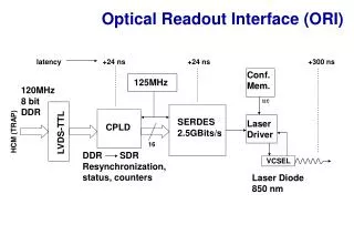
Optical Readout Interface (ORI) • How to push the data out of the FEE? • no handshaking possible • magnetic field • don’t disturb the sensitive PASA Data rate 240 MB/s • because of 8b/10b encoding this means at least 2.4 Gbps • full custom chip started, but not finished at the right time (OASE) • simple board based on commercially available chips • use local high stability quartz oscillator instead of LHC clock • use custom laser driver circuit to avoid using commercial SFP modules with unspecified stability in magnetic field
Optical Readout Interface (ORI) latency +24 ns +24 ns +300 ns Conf. Mem. 125MHz 120MHz 8 bit DDR I2C SERDES 2.5GBits/s Laser Driver CPLD LVDS-TTL HCM (TRAP) 16 DDR SDR Resynchronization, status, counters VCSEL Laser Diode 850 nm Magnetic field & radiation tolerant! All 1200 produced and tested, 1199 of them fully functional
ORI – production test (laser diode) Several parameters controlled: • Supply currents at various operation mode conditions • Voltages on the board in enabled/disabled state • Source, bias and modulation currents through the laser diode • Temperature of the laser driver chip • optical output power • photodiode current measured by the laser driver chip
ORI radiation test in Oslo No permanently damaged components. Equivalent time in years in blue, * - the device fails. Recovery after power cycle or switching off for up to 12 hours (VR and Laser Driver). The configuration of the CPLD and EEPROM was not damaged. Laser DriverLinear Technology LTC5100 100* VCSEL DiodeULM PhotonicsULM850-02-LC-TOSA 20 EEPROM24LC01 30* LVDS TransceiverNational SemiconductorDS90LV048A 30 SerializerTexas InstrumentsTLK2501 250* CPLDLatticeLC4256V 15-50* Voltage RegulatorsNational SemicondutorLP3962-3.3 and -2.5 60-110* F.Rettig
deflection TRD Trigger Timing time bins origin Charge Cluster to Tracklet • Local tracking units on detector perform linear fits and reject uninteresting data Global Tracking • Inside GTU (Global Tracking Unit) • Objective: find high momentum tracks • Search for tracklets belonging together • Combine tracklets from all six layers • Reconstruct pt, compare to threshold and generate trigger • Constraint:only approx. 1.5 µs processing time • Trigger decision after 6 µs • Charge drift and data pre-processing uses most of the time “Tracklet”(32-Bit word): • y position (origin) • slope (deflection) • z position (pad-row number) • charge
Online Track Reconstruction Track Re-assembly • Search for tracklets belonging together(3-dimensional matching task)Projection of tracklets to virtual planeSliding window algorithmA track is found, if ≥ 4 tracklets from different layers inside same multi-dimensional window Reconstruction of the Transverse Momentum • Calculate linear fit of (unprojected)y positions of tracklets. Estimate transverse momentum fromline parameter a uses look-up tables, additions and multiplications Track Projected Tracklets y Virtual Plane x a Module Profile b
GTU in the Framework Pre-Trigger based on TOF, L1 contribution based on GTU Cosmic Trigger Other ALICE Systems TRD Systems GTU CTP L1 contrib, Busy TMUs SMUs TMUs ModifiedTracklet Data TGU SMUs TMUs TTC (L0, L1, L2, …) OnlineTracking Trigger L0 contrib, Busy Other Detectors Outside Magnet T0 TOF Inside Magnet Busy V0 ACORDE Pre-Trigger Pre-Trigger, L0, L1 Szintillators
Storage ORI Global Tracking Unit in the TRD Readout Chain DCSBoardTTCrx TriggerHandling &Control DIU TrackConcentr. DDLSIU RX ORI Event BufferingDesign TriggerDesign TGU CentralTriggerProcessor DATESoftware L1 contribution+ busy • Track Matching Unit (TMU) • Supermodule Unit (SMU) • Trigger Generation Unit (TGU) GTU Racks x 8 1 5x Trackletsonly Half Chamber TTC triggersignals 12 fibres Module Tracklets&Raw Data D - RORC TMU SMU Stack GTU Supermodule Segment Front-End Electronicswithin L3 magnet Racks belowMuon System DAQ System
Event Buffering Design Scheduling MemoryManagement ReadAddressLogic &Control write read 16/128 16/128 SRAMController TMU/SMUInterface DataFormatting Event (n+1, 11) Event (n+1, 0) Event (n, 0) Event (n, 11) Data Block, Link 0 Data Block, Link 11 4-MbitSRAM empty ... 12x ... DataStream Merging data Links from one Stack ... 12x ... Supermodule Unit address Event InfoFIFO Buffer Event Shaper Readout Unit status SMU Control(L0-/L1-Trigger) SMU Control(L2-Message)
Trigger – Simulation Framework AliRoot-based framework of simulation classes:AliEn integration, Offline-RawReader, TRAP/GTU simulation GTU Trigger Model TRD ResponseModel Simulation Framework TMUs SMUs TMUs SMUModels 18 SM, 5 Stacks, 6 Layers, 2 Half-Chambers TMUModels Half-Chamber Models CASTOR/AliEn or Files OfflineRawStream Reader TGUModel Tracklets ADC data TRAP models L1 contrib Trigger Efficiency/Purity Assessment Input of „empty“ and interesting events Configuration parameters
Trigger Schemes Di-Lepton Trigger Tracking developed by Jan de Cuveland Transverse momentum cuts simple coincidence of “high-pt seen flags” from different supermodules Optimized for minimum latency → L1 contribution Jet-Trigger PhD thesis: Concept and Implementation of a Jet trigger in the GTU fast selection of events (L1 contribution) based on thresholds for numbers of high-pt tracks within certain space regions/angular ranges charge sums (if available) within certain space regions/angular ranges more complex calculations (invariant mass, …) and correlationsbeing under consideration currently → idea of L2 contribution by GTU PhD theses on GTU trigger at KIP: S. Kirsch (A-A), F. Rettig (p-p)
Track Matching Unit (TMU) • Trigger design currentlyoptimizedforhighptcutonly • Simple di-leptontriggerforeseen in triggerunit (based on `binary‘ localdecisions)
Track Matching Unit (TMU) Board 3 Parallel Links (240 MHz DDR, 8 Bit LVDS) 850 nm SFP-Transceiver 12 Fiber Optical Serial Links(2.5 GBit/s) Custom LVDS I/O72 Pairs To Right TMU From Left TMU To SMU Board DDR2 SDRAM JTAG 64 MB DDR2 SRAM DDR2 SRAM:High Bandwidth (28.8 GBit/s) Data Buffer From 1 Detector Stack FPGA 4 MB Xilinx XC4VFX100 FF1152 Virtex-4 FX100 FPGA: 95k LCs, 768 I/Os, 20 Internal Multi-Gigabit Serializer/Deserializer Units, 2 PowerPC Cores Config PROM CompactPCI Bus (6U Height, Single Width)
TRD Beam Test at CERN (2007-11) 1 TRD Super-module • Accelerator: CERN Proton Synchrotron (PS) • Particles: Electrons, Pions(Transverse Momenta: 0.5 – 6 GeV/c) • Good statistics for detector calibration (More than 1 Mio. events per momentum value) • 8 days of continuous operation • First run with tracklets, consistent with raw data 1 GTU Segment November 2007 Beam Test Setup at CERN Proton Synchrotron Single Tracklet Deflection Precision Mean: -0.0916 cm RMS: 0.119 cm Count First Tracklets from TRD (not to scale) Deflection Error / cm
Commissioning at CERN /ALICE 2008 Cosmics Runs • Read-out chain running continuously • Writing cosmics data to DAQ via GTU • 60,000 events with pseudo-random test pattern: No errors • Measured TRD readout timing: Fully able to saturate DAQ link TRD Readout Timing • Measured readout time for maximum black event(30 time bins): • L0 → Event at GTU: 245 us (4 kHz)L0 → DDL Tx done: ~ 13 ms (~ 75 Hz)Divide times by a factor of 5–500 for zero-suppressed dataDDL performance: 120 Mbyte/s • DDL utilization: 99 % GTU Installation at CERN (End of 2007, Work in Progress)
SummaryGTU • The TRD Global Tracking Unit (GTU) is the central element of the ALICE TRD trigger system and readout chain • It provides both complex online data analysis within tight low-latency requirements and high bandwidth raw data handling • The GTU system has been fully installed • Commissioning and extensive read-out and interoperability tests have been performed successfully A GTU Segment in Operation • Next steps • Further Tests of the online tracking and trigger functionality • Preparations for first LHC operation in 2008
A Large Ion Collider Experiment • p-p or Pb-Pb Collision • Creation of Quark Gluon Plasma, a state of matter existing during the first few microseconds after the big bang • TRD is used as a trigger detector due to its fast readout time (2 µs): • Transversal Momentum • Electron/Pion Separation Inner Tracking System (ITS) Time Projection Chamber (TPC) Transition Radiation Detector (TRD)
Transition Radiation Detector TRD - Transition Radiation Detector • used as trigger and tracking detector • > 24000 particles / interaction in acceptance of detector • up to 8000 charged particles within the TRD • trigger task is to find specific particle pairs within 6 s. ITS - Inner Tracking System • event trigger • vertex detection TPC - Time Projection Chamber • high resolution tracking detector • but too slow for 8000 collisions / second
Tail Cancellation Filter unfiltered input 12 12 12 filtered output sub 12 13 Long Exponetial Coefficients 15 15 15 15 add register mult add mult 13 13 12 Short Exponetial Coefficients 13 13 13 13 register mult add mult 12
TRAP Layout 8 ch.evt.buf IMEM 2 IMEM 3 13 ch.evt.buf DataBuffer CPU 3 CPU 2 CPU 0 CPU 1 21 ADC Channels Quad Port Memory 21 independent Digital filter channels GRF IMEM 0 IMEM 1 network IF FiFo 5x7 mm