Download
1 / 31
380 likes | 937 Vues
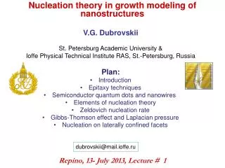
V.G. Dubrovskii St. Petersburg Academic University & Ioffe Physical Technical Institute RAS, St.-Petersburg, Russia. Nucleation theory in growth modeling of nanostructures. Plan: Introduction Epitaxy techniques Semiconductor quantum dots and nanowires Elements of nucleation theory

E N D
V.G. Dubrovskii St. Petersburg Academic University& Ioffe Physical Technical Institute RAS, St.-Petersburg, Russia Nucleation theory in growth modeling of nanostructures • Plan: • Introduction • Epitaxy techniques • Semiconductor quantum dots and nanowires • Elements of nucleation theory • Zeldovich nucleation rate • Gibbs-Thomson effect and Laplacian pressure • Nucleation on laterally confined facets dubrovskii@mail.ioffe.ru Repino, 13- July 2013, Lecture # 1
Modeling of nanostructure formation • Growth theory • Nucleation • Theory of nanostructure formation • Quantum dots • Nanowires • Epitaxial techniques (MBE, MOCVD…) InAs/GaAs(100) QDs Main goals of modeling: • Understanding • Prediction • Optimization • New morphology • New structure • New materials GaAs/GaAs(111)B-Au NWs
Size-dependent quantum effects in nanostructures SE: DOS: Bulk: DOS of nanostructures: Effect on optical properties:
Transformation of QD distribution function into DOS Required properties of NS ensembles: • High uniformity • High density (?) • Controlled composition • Controlled morphology • Controlled crystal structure Morphology of nanostructure ensembles depends on growth process !!!
Technologies of nanostructure formation: MBE and CVD 1. Molecular beam epitaxy = MBE • Developed in early 70s • Now widely used to produce high-quality layers of different • compound semiconductors with very abrupt interfaces and good control • of thickness, doping and composition • Materials are deposited in a form of molecular beams on a heated substrate • Molecular beams are originated from thermally evaporated elemental sources • (effusion cells) • Growth rates are typically of order of several angstroms per second • MBE system consists of 3 main vacuum chambers: • Growth chamber • Buffer chamber (preparation and storage of samples) • Load lock (to bring samples in and out of the vacuum environment) • Rotating samples (manipulator) • Pressure gauge (ion gauge) • Nitrogen cooler • Cryo-pumps, ion pump, turbo pumps to remove gases, residual pressure is • typically less than 10-11 Torr • Substrates holders made from Ta, Mo or pyrolytic boron nitride
Scheme of typical MBE system Monitor residual gases, source beams In situ growth control Deposition • Example for GaAs: • As (As4 or As2 • through a cracker • Ga • Al • In • Be (p-doping) • Si (n-doping) Sample rotation
In situ monitoring by RHEED (continued …) Physical nature of RHHED oscillations
Modern MBE reactors • GaAs growth • 6 x 3 inch substrates • Growth rate 1-3 A/s • 10 sources • As cracking • Two parallel loading • systems • RHEED • QMA • Cryo-panel • 4 standard HEMT • processes daily Riber 49
MOCVD • Metal organic chemical vapor deposition (MOCVD) = MOVPE is being used for • crystal growth from 1960 and in 1980s was applied for the fabrication of • compound semiconductor – based materials and devices • For example, LED structures are grown almost exceptionally by MOCVD • MOCVD systems contain: • the gas handling system to meter and mix reactants • the reactor (vertical or horizontal in design) • the pressure control system • the exhaust facilities • Basic principle is the deposition of the required growth species with precursors • at ~ atmospheric pressure of a carrier gas and chemical reaction in the • temperature field of a heated substrate • Group III sources are trimethylgallium (TMGa), TMAl, TMIn • Group V species are typically hydride gases such as arsine (AsH3) and phoshpine • (PH3), or NH3 for GaN • Very high V/III ratios (50-100) because the incorporation of group V elements • Is self-limited (very high partial pressure of group V species) • Growth rate and composition is controlled by partial pressures of the species and • by the substrate temperature
Chemistry of MOCVD growth process for GaAs Radiofrequency generator (~450 kHz) H2 Source of a metal-organic compound (liquid or solid state) Vapors inH2 Heating up to 600-7000С Chemical reaction Hydrides (gaseous) Example of chemicalreaction for the GaAs epitaxy: Growth of compound semiconductor on a crystal substrate H2 (CH3)3Ga + AsH3 GaAs + 3CH4 6000C Exhaust of gases
Modern MOCVD reactors (1-x)Ga(CH3)3 + xIn(CH3)3 + NH3 -> InxGa1-x N + 3CH4 ReactorAixtron 2000/HT (2003):GaN growth 6 x 2-inchsubstrates Productivity > 500 blue LED structures monthly Each wafer contains ~ 10 000 LED chips 0.35*0.35 mm
Heterostructres for blue-green and white LEDs • Main technological stages: • Wafers Al2O3 • Materials (TMGa, TMAl,TMIn, gases) • Epitaxial growth of LED heterostructure • Processing and production of chips • Packaging • Fabrication of final device Increasing In concentration in InGaN => larger wavelength
Direct formation of Stranski-Krastanow QDs 20 nm Relaxation of elastic stress in the island – main driving force for 2D-3D transition SK growth mode
Direct formation of QDs (continued …) At h=h1c, RHEED pattern changes from strikes to spots 2 ML InAs/GaAs Coherent stained islands Dislocations ε0>2% Critical thickness h1c for 2D-3D transition
VLS growth of “whiskers” by Wagner & Ellis and Givargizov Wagner & Ellis, APL 1964 Пар-жидкость-кристалл или ПЖК (в английской литературе — vapor-liquid-solid — VLS)) — механизм роста одномерных структур, таких как нановискеры в процессе химического осаждения из газовой фазы. High temperature (T ~ 1000-11000 C) CVD experiments of 1960-70s with micrometer diameters
Formation of vertical nanowires on activated surfaces by MBE GaAs/GaAs(111)B-Au 1-st stage (MBE chamber): oxide desorption from GaAs substrate and buffer layer growth GaAs wafer Au film 2-st stage (Vacuum or MBEchamber): Au deposition on a GaAs substrate surface GaAs wafer GaAs NW 3-st stage (MBE chamber): formation of Au-Ga alloy droplets; deposition of GaAs – growth of NW GaAs wafer
200 nm GaAs/GaAs(111)B Typical RHEED patterns during the wire growth 200 nm GaAs/Si(100)
ZB and WZ phase of III-Vs All III-V NWs, except nitrides, have STABLE ZB cubic phase in BULK FORM In GaAs: Difference in cohesive energies = 16. 6 – 24 meV per pair at zero ambient pressure. T.Akiyama et al, Jpn.J.Appl.Phys, 2006; M.I.McMahon and R.J.Nelmes, PRL, 2005 Bulk ZB GaAs becomes unstable at pressure ~ 80 GPa !!! ABC=ccc=3C=∞ ABA=hhh=2H=(11) Most of ZB III-V nanowires contain WZ phase: A.I.Person et al., Nature Materials 2004, Au-assisted MOVPE of III-V/III-V J.C.Harmand et al., APL 2005, Au-assisted MBE of GaAs/GaAs I.P.Soshnikov et al., Phys. Sol. State 2006, Au-assisted MBE of GaAs/GaAs P.Mohan et al., Nanotechnology 2005, selective area catalyst free growth of III-Vs C.Chang-Hasnain group, Au-assisted MOCVD of III-V/Si AND MANY OTHERS!
Hexagonal WZ phase in III-V NWs !!! LPN CNRS: APL 2005 InAs NWs on InAs GaAs NWs on GaAs [1 1 0 0] zone axis C. Chang-Hasnain, group: 0002 0000 APL 2007 1120 InP NWs on Si TEM image FFT of TEM image
ZB-WZ transition in GaAs NWs (Ioffe & LPN) Au-assisted MBE of GaAs on the GaAs(111)B substrate ZB Switching from WZ to ZB at the end of growth WZ I.P.Soshnikov et al, Phys. Sol. State 2005 Switching from ZB to WZ at the beginning of growth ZB phase systematically appears at low supersaturation ! F.Glas et al., Phys. Rev. Lett 2007
Consider 2D island of ML height h, area A=c1r2and perimeter P=c2r, r = “radius” Gibbs free energy of 2D island formation (fixed T, P, N): Nucleation (1a) in kBT units Difference in chemical potentials (energetically favorable) Surface term (energetically unfavorable) i Surface energy constant A=s i γ – solid-vapor surface energy per unit area (J/m2) Δμ– difference of chemical potentials (J) Normally, a is a large parameter ~ several tens g h
Gibbs free energy Activation barrier for nucleation: n=10-3 , a=15 =0.75 (1), 1 (2), 1.5 (3) and 2 (4). Critical number of atoms: F ic Half-width near maximum: F and icdecrease as supersaturation increases !!!
A story about Zeldovich and nucleation theory ФИЗИЧЕСКИЕ ОСНОВЫ ТЕОРИИ ФАЗОВЫХ ПРЕВРАЩЕНИЙ ВЕЩЕСТВА (КУНИ Ф.М. , 1996), ФИЗИКА Сформулированы цели современной теории фазовых превращений, введены понятия о стабильных и нестабильных фазах вещества, образовании зародышей стабильной фазы в недрах метастабильной, вероятностно-статистическое представление о потоке зародышей как о ведущей кинетической характеристике фазового превращения. Описана временная зависимость фазового превращения (уравнение Зельдовича???). Я.Б. Зельдович
Nucleation rate Region 1:Equilibrium size distribution exp(F)>>1 I – nucleation rate [1/cm2s] Region 2:Fluctuations [ flux I] F dic/dt=0 Region 3:Growth f(i,t) – island size distribution [1/cm2] I III II Kinetic equation for size distribution in region II: i ic-Δic ic ic+Δic Boundary conditions:
Nucleation rate (continued…) Stationary solution at J=const with the 2nd boundary condition: J=0 equilibrium J=const steady state To meet the 1st boundary condition, I should equal: i+1 i Laplace method i-1 General Zeldovich formula for 2D islands
Gibbs-Thomson effect and Laplacian pressure Consider liquid (L) spherical drop of radius R in equilibrium with vapor (V) PV Find PL-PV, PLand PV R PL Solution: γ 1) System at fixed T, V and μ => maximum of at constant volume For a sphere with Laplacian surface pressure yields For a cylindrical isotropic solid with
GT effect and Laplaciam pressure (continued …) 2) At finite R, equilibrium state is defined by (1) (2) At R→∞, equilibrium state is defined by Subtract (1) from (2); take into account that liquid is incompressible and that vapor is ideal Vapor: Liquid:
Mononuclear and polynuclear growth I – nucleation rate, v=dr/dt – 2D island growth rate, R – face radius I and v are time-independent during growth (constant supersaturation) Polynuclear growth is generally faster ! VL= vertical growth rate of facet of radius R due to 2D nucleation VL Generally, VL=f(I,v,R) R R Kashchiev interpolation formula: Dependence on the nucleation barrier:
A story about Kolmogorov-Mehl-Johnson-Avrami model Википедия: Уравнение Джонсона — Мела — Аврами — Колмогорова (англ.Johnson — Mehl — Avrami — Kolmogorov equation, JMAK) описывает процесс фазового перехода при постоянной температуре. Изначально оно было получено для случая кристаллизациирасплавов в 1937 году А. Н. Колмогоровым, и независимым образом в 1939 году Р. Ф. Мелом и У. Джонсоном, а также было популяризировано в серии статей М. Аврами в 1939—1941 годах. A. Kolmogorov