The ATLAS IBL Project
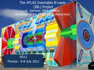
The ATLAS IBL Project. The 5 th "Trento" Workshop on Advanced Silicon Radiation Detectors Manchester, 24-26 February 2010 G. Darbo - INFN / Genova Conference Site: http://www.hep.man.ac.uk/Radiation-Detectors2010/agenda.html. ATLAS Pixel Detector. ATLAS Pixel Detector

The ATLAS IBL Project
E N D
Presentation Transcript
The ATLAS IBL Project The 5th "Trento" Workshop on Advanced Silicon Radiation Detectors Manchester, 24-26 February 2010 G. Darbo - INFN / Genova Conference Site: http://www.hep.man.ac.uk/Radiation-Detectors2010/agenda.html
ATLAS Pixel Detector ATLAS Pixel Detector • 3 Barrel + 3 Forward/Backward disks • 112 staves and 48 sectors • 1744 modules • 80 million channels
The ATLAS Pixel Module ATLAS Pixel Module • 16-frontend chips (FE-I3) modules with a module controller chip (MCC) • 47232 pixels (46080 R/O channels), 50 x 400 µm2 (50 x 600 µm2 for edge pixel columns between neighbour FE-I3 chips) • Planar n-on-n DOFZ silicon sensors, 250 µm thick • Designed for 1 x 10¹⁵ 1MeV fluence and 50 Mrad • Opto link R/O: 40÷80 Mb/link
IBL: Project History • The ATLAS Pixel B-Layer initially designed for replacement • September 2007 B-Layer replacement Workshop outcome: replacement not possible in 1 year shutdown. • January 2008: ATLAS Task Force (A. Clark & G. Mornacchi) Report July 2008 (Bern): preferred (only) option Insertable B-Layer (IBL) • February 2009: project approved by ATLAS May 2009 IBL management organization in place. • Now: design fast advancing, IBL Technical Design Report (TDR) draft, interim Memorandum of Understanding (i-MoU) in discussion. • Mission impossible… fit an additional layer in between Pixel and beam-pipe: • Reduce beam-pipe by 4 mm in radius… and make it possible! IouriiGusakov Existing B-Layer IBL
Motivation for IBL • The existing B-Layer cannot be replaced in a long LHC shutdown (8-months): • This was a major finding of the B-Layer task force. Many reasons make it very difficult: • Extraction, moving to surface and opening the whole Pixel Detector package. • Work on an activated material. • Risk of damage (many last moment operations made the process “irreversible” in the final phase of the detector integration). Reasons for an IBL to back-up existing B-Layer: • Radiation damage • Sensor and electronics degradation of the existing B-Layer reduce detector efficiency after 300÷400 fb-1 (last forecast of LHC integrated luminosity move it more far away) • Insurance for hard failures in the Pixel B-Layer • The Pixel Detector cannot be repaired in case of cooling, opto-links, module hard failure. Inefficiencies of the B-layer have high impact on many Physics channels. • Improve existing B-Layer Physics performance • A low mass detector (~50% of existing B-Layer) improves Physics performance.
IBL Layout • Beam-pipe reduction: • Inner R: 29 25 mm • Very tight clearance: • “Hermetic” to straight tracks in Φ (1.8º overlap) • No overlap in Z: minimize gap between sensor active area. • Layout parameters: • IBL envelope: 9 mm in R • 14 staves. • <R> = 33 mm. • Z = 60 cm (active length). • η = 2.5 coverage.
BP Extraction & IBL+BP Insertion Ref.: Y.Gusakov, N.Hartman, R.Vuillermet • Material from Raphael/Neal • The present 7m long section of the beam-pipe will be cut (flange too big to pass inside the existing pixel) and extracted in situ: • The new beam-pipe with the IBL will be inserted at its place: • A carbon tube (IST) is inserted before the IBL: to support the new detector and to simplify the insertion procedure. PP1 Collar Sealing service ring Alignment wirers IST IBL Support Tube Stave Stave Insert To fix to support, survey reference
B-Layer Scenarios Physics performance studies ongoing for the IBL TDR (ATHENA/GEANT4). Preliminary studies (ATLSIM/GEANT3) show improved performance with the addition of IBL (see low mass Higgs b-jet tagging plot on the right). Performance improvement due to low mass and smaller radius: Aggressive reduction of material budget is a must! WH(120 Gev) SV1 εb=60% Light jets rejection SV1 εb=70% 2-layers R=3.5 cm and 8 cm 2-old layers ATLAS b-inserted as 4-layer R=3.5 cm b-replaced (*) Material budget used in the simulation Ref.: A. Rozanov
Requirements for Sensors/Electronics • Requirements for IBL • IBL design peak luminosity = 3x1034 cm-2s-1 FE-I4 architecture & R/O bandwidth: must be understood after Chamonix • Integrated luminosity seen by IBL = 550 fb-1 Survive to sLHC phase II • Design sensor/electronics for total dose: • NIEL dose = 3.3 x 10¹⁵ ± (“safety factors”) ≥ 5 x 10¹⁵ neq/cm2 • Ionizing dose ≥ 250 Mrad • Fit made for 2 < r < 20 cm for L=550fb-1 • Gives for IBL @ 3.2 cm (550 fb-1): • Φ1MeV=3.3x10¹⁵ neq/cm2 (1.6 MGy) • Safety factors not included in the computation (σppevent generator: 30%, damage factor for 1 MeVfluences: 50%) Ref.: Ian Dawson
FE-I4 Architecture: Obvious Solution to Bottleneck • >99% or hits will not leave the chip (not triggered) • So don’t move them around inside the chip! (this will also save digital power!) • This requires local storage and processing in the pixel array • Possible with smaller feature size technology (130 nm) • Large chip - design methodology: • Custom digital layout substituted by automatic place & route of synthesized design. • Chip verification is the challenge: analog/digital and mix-mode test bench simulation. FE-I3 @ R = 5 cm Ref.: M. Barbero et al.
FE-I3 FE-I4 FE-I4 Collaboration: Bonn: D. Arutinov, M. Barbero, T. Hemperek, A. Kruth, M. Karagounis. CPPM: D. Fougeron, M. Menouni. Genova: R. Beccherle, G. Darbo. LBNL: S. Dube, D. Elledge, M. Garcia- Sciveres, D. Gnani, A. Mekkaoui. Nikhef: V. Gromov, R. Kluit, J.D. Schipper The first version of full FE-I4 chip will be submitted by end of March 2010 ~70 million transistors, 0.13 µm CMOS technology 6 Cu and 2 Al routing layers. 20.2mm ~200μm 7.6mm ~19 mm active IBM reticule 16.8mm 8mm active 2.8mm ~2mm Chartered reticule (24 x 32) FE-I3 74% FE-I4 ~89%
The Way to FE-I4: Test Chips FE-I4-P1 3mm SEU test IC LDORegulator 61x14 array Control Block ShuLDO+trist LVDS/LDO/10b-DAC ChargePump 4-LVDS Rx/Tx CapacitanceMeasurement low power discriminator CLKGEN proto: PLL core + PRBS + 8b10b coder + LVDS driv 4mm DACs CurrentReference
FE-I4 4-pixel region analog 1-pixel pixel array 336×80 pixels digital4-pixel region periphery
FE-I4: The Pixel Cell Ref.: A. Mekkaoui 2-stage architecture optimized for low power, low noise, fast rise time. • regular cascode preamp. NMOS input. • folded cascode 2nd stage PMOS input. • Additional gain, Cc/Cf2 ~6. • 2nd stage decoupled from leakage related DC voltage shift. • Cf1 ~17 fF (~4 MIPs dynamic range). 150 µm 13-bit memory/pixel: 4 FDAC, 5 TDAC, 2 cap, 1 HitEN, 1 HitOR
Noise and Radiation Results ENC @ Low Current (10µA) • ENC on “Collaboration Proto 1” before and after irradiation (200 Mrad) • Measured ENC for pixels with and without Cload • Simulated ENC and time-walk @ 10 µA/pixel (preamp + amp2 + comparator) 200Mrad, Cload~400fF a) ENC[e-] c) ENC=160e- @ Cd=0.4pF & IL=100nA 150 (10 µA) tLE[s] IL=100 nA 20n b) 100 IL = 0 nA 60 100f 200f 300f Cd[F] 10n (loaded ~400 fF) 20 ns timewalk for2 ke- < Qin < 52 ke-& threshold @ 1.5 ke- <ENC> ~ 90 e <ENC> ~ 65 e 0 Qin[C] 20k 30k 40k 10k
Module Design: Sensor Technology Independent • Decision onsensors after TDR • Need module prototypes with FE-I4 (second half 2010) • Common sensor baseline for engineering and system purposes • 3D / Diamond sensors – single chip modules / Planar sensors – 2 chip modules • Sensor/module prototypes for ~10% of the detector in 2010 • Stave prototype tested with modules and cooling Single chip module: Edge < 325 µm Double chip module: Edge < 450 µm Credits: M.Garcia-Sciveres – F. Hügging
Sensors • 3 sensor technologies considered for IBL • Planar, 3D and Diamonds • Full scale prototypes with FE-I4 – Decision on spring 2010 • Some specifications agreed: • Max fluence > 5 x 10¹⁵ 1MeV neutrons / cm2 • Max power after full life dose < 200 mW/cm2 • Low dead area in Z: slim or active edge • Maximum bias voltage (system issue) : 1000 V • Sensor R&D and prototype work for IBL are presented in many talks in the Workshop…
Bump Bonding • Large volume bump-bonding experience from Pixel Detector (see table): • PbSn and Indium bumps: PbSnAgSn • Program to qualify for the larger FE-I4 and different sensor technologies. • Setting up with mechanical/electrical dummies, but finally real parts needed: thermo-mechanical process strongly dependent on actual metal layers of electronic chip and sensor. • Goal to go below 190 µm of the Pixel Detector: target to 90 µm. “dummy – sensor” (monitor wafer) Prototype test of advanced AgSn bumping with 90µm FE-I4 size dummies. ATLAS Pixel bump-bonding production – Ref: Jinst 3 P07007 (2008)
Thermal Figure of Merit and Thermal Run-away Thermal runaway happens in sensors if not adequately cooled • Leakage current shows exponential behavior. Stave thermal figure of merit (Γ=[ΔT•cm2/W]) main parameter for thermal performance. Power design requirements for IBL: Sensor Power 200 mW/cm2 @ -15 C FE power 400 mW/cm2 Stave prototype qualification program: Titanium / carbon fiber pipes (D = 2÷3 mm) Cooling CO2 and C3F8 Carbon foam density: 025÷0.5 g/cm3 Radiation length: 0.36÷0.66 %X/X0 Pipe + stave structure + coolant Thermal Runaway Plot Evaporation T = -40 ºC = 30.0 C•cm2/W = 18.5 C•cm2/W = 3.2 C•cm2/W IBL including safety Ref.: D Giugni, H. Pernegger, M. Gilchriese
Stave Structure Stave structure made of carbon foam + cooling pipe (carbon fiber or titanium boiling channel) • The stiffness is provided by a carbon fiber laminate: Fiber YS-80A; resin EX-1515; lay-up (0/60/-60)S2 • Carbon foam diffuses the heat from the module to the cooling pipe Poco Foam r=0.55g/cm3; K=135/45 W/mKOR KopersKFOAM L1-250 r=0.245g/cm3; K=30 W/mK Module (sensor + bumps + FE-I4) Carbon foam Omega CF laminate Ti or CF pipe
Stave Prototype Options • Additional technical requirements (prototype work) • Max pressure of cooling pipe: 100 bar. • Develop pipe joints and fittings. • Gravitational / thermal deformation < 150 µm. • Isolation of the carbon foam from sensor high voltage. • Mock-up for thermal measurements. Module parameters • Sensor thickness = 250 µm • FE-I4 thickness = 90 µm • Flex Hybrid (η = 0) = 0.18 % of X0 Carbon Foam 0.25g/cm3
When IBL in ATLAS? • IBL plans to be ready for installation by end of 2014. • Cannot be much before without compromising performance • A shut down of the machine of 8 month needed (4 to open/close ATLAS) • LHC plans after Chamonix are not clear: how peak and integrated luminosity increase and when machine shutdown will be scheduled: • Only plans up to 2012 are known. • Many LHC upgrades need shutdowns: • Linac4, Collimators phase II, new interaction region quadrupole triplets, etc. • Probably in one year from now we will know next 5 years plans. • Chamonix Agenda: • http://indico.cern.ch/conferenceDisplay.py?confId=67839 • Summary of the Chamonix Workshop at Cern: • http://indico.cern.ch/conferenceDisplay.py?confId=83135 IBL
Conclusions • IBL will improve physics performance of ATLAS and it is a “safety insurance” for present B-Layer • TDR and MoU in progress – project cost evaluated • Motivated groups and institutes support • Challenging project: • Tight envelopes, material budget reduction, radiation dose and R/O bandwidth requirements • New technologies in advanced prototype phase: • FE-I4, light supports, cooling, but mainly… SENSORS !!!
Installation Scenarios R. Vuillermet • Two global support / installation scenarios: IBL support tube (1) / no tube (2): • An IBL support tube would have advantage on stiffness and simplicity/safety for IBL installation, but drawback are envelope needs (~1÷1.5 mm) and increase of radiation length • Procedure studied on mock-up at bld.180 - procedure (1) animation: • The beam pipe flange on A-side is to close to the B-layer envelope - Need to be cut on the aluminum section • A structural pipe is inserted inside the Beam Pipe and supported at both sides. • The support collar at PP0 A-side is disassembled and extracted with wires at PP1. • Beam pipe is extracted from the C-side and it pulls the wire at PP1 • New cable supports are inserted inside PST at PP0. • A support carbon tube is pushed inside the PST along the structural pipe. • The support carbon tube is fixed in 2 point of PP0 and on PP1 walls on side C and A. • The structural pipe with a support system is moved out from the support carbon tube. . The new beam pipe (in any configuration with OD up to 82,5 mm) is inserted from A-side. It has 2 supports at PP0 area and 2 floating wall at PP1 on side A and C. C-side A-side Started to setup a 1:1 mock-up of Pixel/beampipe/PP1 in Bat 180
IBL Organisation Structure • Membership • IBL Project Leader: G. Darbo • IBL Technical Coordinator: H. Pernegger • “Module” WG (2 Physicists): F. Hügging & M. Garcia-Sciveres • “Stave” WG (1 Phy. + 1 M.E.): O. Rohne + D. Giugni • “IBL Assembly & Installation” WG (2 M.E. initially, a Phy. Later): N. Hartman + R. Vuillermet • “Off-detector” WG (1 Phy. + 1 E.E.): T. Flick + S. Débieux • “Extra” members: • Ex officio: Upgrade Coordinator (N. Hessey), PO Chair (M. Nessi), Pixel PL (B. Di Girolamo), ID PL (P. Wells), Pixel Chair (C. Gößling) • Offline “liaison” Pixel Off-line coordinator: A. Andreazza • TDR editor (temporary): K. Einsweiler • Whole project divided into 4 working groups • IBL Management Board has 10 members, plus “extra” and ex-officio members. • Frequent meetings (every ~14 days) in this phase of the project. • IBL Management Board • Membership: • IBL PL + IBL TC • 2 coordinators from each WG • Plus “extra” members • Module WG • (2 coordinators) • FE-I4 • Sensors • Bump-Bonding • Modules • Test & QC • Irradiation • Stave WG • (1 Phys + 1 Eng.) • Staves • Cooling Design & Stave Thermal Management • HDI • Internal Services • Loaded Stave • Test & QC • IBL Integr.-Install. • (2 Eng.) • Stave Integration • Global Sup. • Beam Pipe (BP) • Ext.services inst. • IBL+BP Installation • Cooling Plant • Test & QC • Off-detector • (1 Phys + 1 E.Eng.) • Power • DCS • ROD • Opto-link • Ext.serv.design/proc. • Test Beam • System Test

