Download
1 / 18
180 likes | 203 Vues
Learn how to design a single-cycle CPU with detailed steps including analyzing instruction set architecture, assembling datapath components, and implementing control logic.

E N D
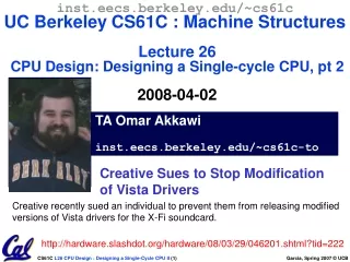
inst.eecs.berkeley.edu/~cs61cUC BerkeleyCS61C : Machine StructuresLecture 26CPU Design: Designing a Single-cycle CPU, pt 22008-04-02 TA Omar Akkawi inst.eecs.berkeley.edu/~cs61c-to Creative Sues to Stop Modification of Vista Drivers Creative recently sued an individual to prevent them from releasing modified versions of Vista drivers for the X-Fi soundcard. http://hardware.slashdot.org/hardware/08/03/29/046201.shtml?tid=222
How to Design a Processor: step-by-step 1. Analyze instruction set architecture (ISA) => datapath requirements • meaning of each instruction is given by the register transfers • datapath must include storage element for ISA registers • datapath must support each register transfer 2. Select set of datapath components and establish clocking methodology 3. Assemble datapath meeting requirements 4. Analyze implementation of each instruction to determine setting of control points that effects the register transfer. 5. Assemble the control logic
Clocking Methodology Clk • Storage elements clocked by same edge • Being physical devices, flip-flops (FF) and combinational logic have some delays • Gates: delay from input change to output change • Signals at FF D input must be stable before active clock edge to allow signal to travel within the FF (set-up time), and we have the usual clock-to-Q delay • “Critical path” (longest path through logic) determines length of clock period . . . . . . . . . . . .
ALU Register-Register Timing: One complete cycle Clk New Value Old Value PC Instruction Memory Access Time Rs, Rt, Rd, Op, Func Old Value New Value Delay through Control Logic ALUctr Old Value New Value RegWr Old Value New Value Register File Access Time busA, B Old Value New Value ALU Delay busW Old Value New Value ALUctr RegWr Rd Rs Rt Register Write Occurs Here 5 5 5 busA 32 Rw Ra Rb busW 32 RegFile busB 32 clk
op rs rt 31 16 15 0 immediate 0 0 0 0 0 0 0 0 0 0 0 0 0 0 0 0 16 bits 16 bits ALU 3c: Logical Operations with Immediate • R[rt] = R[rs] op ZeroExt[imm16] ] 31 26 21 16 0 immediate 6 bits 5 bits 5 bits 16 bits But we’re writing to Rt register?? ALUctr RegWr Rd Rs Rt 5 5 5 busA 32 Rw Ra Rb busW 32 RegFile busB 32 clk
op rs rt 31 16 15 0 immediate 0 0 0 0 0 0 0 0 0 0 0 0 0 0 0 0 16 bits 16 bits ALU 3c: Logical Operations with Immediate • R[rt] = R[rs] op ZeroExt[imm16] ] 31 26 21 16 0 immediate 6 bits 5 bits 5 bits 16 bits RegDst Rd Rt What about Rt register read?? 1 0 RegWr Rs Rt ALUctr 5 5 5 busA 32 Rw Ra Rb 32 RegFile busB 32 0 32 clk imm16 1 ZeroExt 16 32 ALUSrc • Already defined 32-bit MUX; Zero Ext?
31 26 21 16 0 op rs rt immediate 6 bits 5 bits 5 bits 16 bits ALU 3d: Load Operations • R[rt] = Mem[R[rs] + SignExt[imm16]] Example: lw rt,rs,imm16 RegDst Rd Rt 1 0 RegWr Rs Rt ALUctr 5 5 5 busA 32 Rw Ra Rb 32 RegFile busB 32 0 32 clk imm16 1 ZeroExt 16 32 ALUSrc
31 26 21 16 0 op rs rt immediate 6 bits 5 bits 5 bits 16 bits 1 0 ALU 0 1 3d: Load Operations • R[rt] = Mem[R[rs] + SignExt[imm16]] Example: lw rt,rs,imm16 MemtoReg ALUctr RegDst Rd Rt MemWr RegWr Rs Rt 5 5 5 busA 32 Rw Ra Rb busW 32 RegFile busB 32 0 32 clk ? 32 WrEn Adr imm16 Data In 1 Extender Data Memory 16 32 clk ALUSrc ExtOp
31 26 21 16 0 op rs rt immediate 6 bits 5 bits 5 bits 16 bits 1 0 ALU 0 1 3e: Store Operations • Mem[ R[rs] + SignExt[imm16] ] = R[rt] Ex.: sw rt, rs, imm16 MemtoReg ALUctr RegDst Rd Rt MemWr RegWr Rs Rt 5 5 5 busA 32 Rw Ra Rb busW 32 RegFile busB 32 0 32 clk 32 WrEn Adr imm16 Data In 1 Extender Data Memory 16 32 clk ALUSrc ExtOp
31 26 21 16 0 op rs rt immediate 6 bits 5 bits 5 bits 16 bits 1 0 ALU 0 1 3e: Store Operations • Mem[ R[rs] + SignExt[imm16] ] = R[rt] Ex.: sw rt, rs, imm16 MemtoReg ALUctr RegDst Rd Rt MemWr RegWr Rs Rt 5 5 5 busA 32 Rw Ra Rb busW 32 RegFile busB 32 0 32 clk 32 WrEn Adr imm16 Data In 1 Extender Data Memory 16 32 clk ALUSrc ExtOp
31 26 21 16 0 op rs rt immediate 6 bits 5 bits 5 bits 16 bits 3f: The Branch Instruction beq rs, rt, imm16 • mem[PC] Fetch the instruction from memory • Equal = R[rs] == R[rt] Calculate branch condition • if (Equal) Calculate the next instruction’s address • PC = PC + 4 + ( SignExt(imm16) x 4 ) else • PC = PC + 4
31 26 21 16 0 op rs rt immediate 6 bits 5 bits 5 bits 16 bits 00 PC Datapath for Branch Operations • beq rs, rt, imm16 Datapath generates condition (equal) Inst Address Equal nPC_sel 4 ALUctr RegWr Rs Rt Adder 5 5 5 busA 32 Rw Ra Rb = busW 32 Mux RegFile ALU busB Adder 32 clk clk PC Ext Already have mux, adder, need special sign extender for PC, need equal compare (sub?) imm16
Inst Memory Adr Adder Adder Mux 1 0 = 00 ALU 0 PC 0 WrEn Adr 1 1 Extender Data Memory PC Ext Putting it All Together:A Single Cycle Datapath Instruction<31:0> <0:15> <21:25> <16:20> <11:15> Rs Rt Rd Imm16 RegDst nPC_sel MemtoReg ALUctr Rd Rt Equal MemWr RegWr Rs Rt 4 5 5 5 busA 32 Rw Ra Rb busW 32 RegFile busB 32 32 clk 32 clk imm16 Data In 16 32 clk imm16 ExtOp ALUSrc
ALU An Abstract View of the Implementation Control Ideal Instruction Memory Control Signals Conditions Instruction Rd Rs Rt 5 5 5 Instruction Address A Data Addr Data Out Rw Ra Rb 32 32 Ideal Data Memory 32 Register File PC Next Address B Data In clk clk clk 32 Datapath
ALU An Abstract View of the Critical Path Critical Path (Load Instruction) = Delay clock through PC (FFs) + Instruction Memory’s Access Time + Register File’s Access Time, + ALU to Perform a 32-bit Add + Data Memory Access Time + Stable Time for Register File Write Ideal Instruction Memory Instruction (Assumes a fast controller) Rd Rs Rt 5 5 5 Instruction Address A Data Addr Rw Ra Rb 32 32 Ideal Data Memory 32 Register File PC Next Address B Data In clk clk clk 32
Administrivia • Authnews is back up! • The server for off-campus newsgroup access was down for a few days, but it’s back up now, so resume using it. • Project 1 grading is being looked into. • Many students have had questions about grades for project 1, so the TAs in charge of project 1 are investigating it. Stay tuned for further announcements. • Homework 6 due Saturday.
Peer Instruction ABC 0: FFF 1: FFT 2: FTF 3: FTT 4: TFF 5: TFT 6: TTF 7: TTT Our ALU is a synchronous device We should use the main ALU to compute PC=PC+4 The ALU is inactive for memory reads or writes.
Instruction<31:0> instr fetch unit nPC_sel <0:15> <21:25> <16:20> <11:15> clk Rs Rt Rd Imm16 1 0 = ALU 0 0 WrEn Adr 1 1 Extender Data Memory Summary: A Single Cycle Datapath • We have everything except control signals RegDst Rd Rt ALUctr MemtoReg RegWr Rs Rt zero MemWr 5 5 5 busA 32 Rw Ra Rb busW 32 RegFile busB 32 32 clk 32 imm16 Data In 16 32 clk ExtOp ALUSrc