
R&D for future detectors
R&D for future detectors. Detectors. Silicon based detectors Vertexing for Linear Collider Silicon Pixel sensors – MAPs, HAPs, CCD, Depfet Tracking for Linear Collider Silicon drift High radiation environments Lazarus, 3d detectors Micropattern gas detectors

R&D for future detectors
E N D
Presentation Transcript
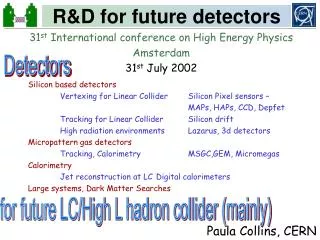
R&D for future detectors Detectors Silicon based detectors Vertexing for Linear Collider Silicon Pixel sensors – MAPs, HAPs, CCD, Depfet Tracking for Linear Collider Silicon drift High radiation environments Lazarus, 3d detectors Micropattern gas detectors Tracking, Calorimetry MSGC,GEM, Micromegas Calorimetry Jet reconstruction at LC Digital calorimeters Large systems, Dark Matter Searches 31st International conference on High Energy Physics Amsterdam 31st July 2002 for future LC/High L hadron collider (mainly) Paula Collins, CERN
You have been weighed in the balance And your X0 is too large LC physics demands excellent Vertexing (b,c,t) and Tracking a in a high B field a with energy flow LEP LEP vs LC by Rembrandt At LC: “x sections are tiny” “No radiation issues” “Triggerless operation possible” “Modest rates” Why not use a LEP/SLD detector?
Time Silicon for vertexing @ the LC required performance disentangle complex events Train • Use a silicon based pixel detector • Confine the e+e- background with a high solenoidal field • Keep occupancy reasonable by reading inner layer in 50 msec discriminate b from c and from background d (IP) < 5 mm 10 mm/(p sin3/2q) (best SLD 8 mm 33 mm/(p sin3/2q)) Vertex detector characteristics point resolution 1-5 mm Thickness ~ 0.1 % X0 5 layers Inner radius ~ 1.5 cm
Silicon Trends Basic idea amplifier • Start with high resistivity silicon • More elaborate ideas: • n+ side strips – 2d readout • Integrate routing lines on detector • Floating strips for precision Al strip p+ + + SiO2/Si3N4 - - + n bulk + n+ - + Vbias Hybrid Active Pixel Sensors Chip (low resistivity silicon) bump bonded to sensor Floating pixels for precision chip chip n+ p chip n+ DEPFET: Fully depleted sensor with integrated preamp chip MAPS: standard CMOS wafer Integrates all functions CCD: charge collected in thin layer and transferred through silicon
15 V 0V 0V + + + DEPFET sensors Kemmer, Lutz, 1987 R&D for tracking ~ 2000 300 mm + Image of toothed watch wheel Resolution: 9 mm (50 mm pixels) • Amplifying transistor integrated into high resistivity silicon detector • Low noise operation possible at room temperature • Thinning possible to 50 mm NIMA 465 (2001) 247-252 R&D: pixel size, power, thinning, speed End 2002: 128x128 30mmx30mm prototypes
Monolithic Active Pixel Sensors (MAPS) 1999 – R&D on CMOS MAPS 1999 – small scale prototypes 1999-2000 first beam tests 2001 – large prototypes • Same unique substrate for detector and electronics • No connections (e.g. bumps) • Radiation hardness (no bulk charge transfer) • Advantages of CMOS process: Easy Design/good yield/low power/Rad hard • Very small pixel sizes achieveable ~ 15 mm Mimosa I II III IV V VI Process 0.6 mm 0.35 mm 0.25 mm 0.35 mm 0.6 mm 0.35 mm Epi layer 14 mm 4.2 mm 2.3 mm 0 (!!!) 14 mm 4.2 mm # pixels 64x64x4 64x64x6 128x128x2 64x64x4 1,000,000x7 24x128x..
MAPS Beam Test Results Signal to Noise Resolution [mm] MIMOSA V MIMOSA I MIMOSA I MIMOSA II MIMOSA V Resolution 1.4 mm 2.2 mm 1.7 mm Efficiency at S/N > 5 99.5 % 98.5 % 99.3% Irradiation of MIMOSA I & II up to 1013 1 MeV/c neutrons Gain a constant Noise a constant Leakage current a moderate rise collected charge a 50-70% of initial value (smooth decrease after 1012 or few x 1011 ) NIMA 478 (2002) 311-315
Charged Coupled Devices - CCDs CCDs invented in 1970 – widely used in cameras, telescopes etc. Tracking applications for HEP: 1980-1985 NA32 120 kpixels 1992-1995 SLD 120 Mpixels 1996-1998 SLD upgrade 307 Mpixels TESLA 799 Mpixels ~1000 signal electrons are collected by a combination of drift and diffusion over a ~20mm region just below surface 10V 2V • Small pixel size – 20 x 20 mm • Possibility of very thin detectors • Column parallel readout: serial register -> direct bump bonding to chip
Layer Radius (mm) CCD lxw (mm x mm) CCD Size (Mpix) Clock / readout time Background (Hits/mm2) Integrated background (kHits/train) 1 15 100 x 13 3.3 50 MHz/50 ms 4.3 761 5 60 125 x 22 6.9 25 MHz/250 ms 0.1 28 CCD R&D for LC requirements • Speed up readout • 5 MHz readout -> 50 MHz • Reduce clock amplitudes 10V->3V • Build with high resistivity epitaxial material • Study radiation resistance to LC doses of 100Krad ionising radiation + 5 x 10⁹ neutrons • Temperature dependence • Minimise material in fiducial volume • Highly thinned silicon glued to substrate • Unsupported “stretched silicon” option CCD 55Fe spectrum: 50MHz 3V clocks noise=2.8 counts lcfi proposal: April 2002
Integration into LC design • Baseline design • 5 layers • R_min=15 mm • 3 layer coverage to |cos q|=0.96 • 5 layer coverage to |cos q|=0.9 Cryostat for CCD option flavour tagging performance at s=91 GeV Purity • b jets roughly equal SLD performance • c jets improved by factor 2-3 in efficiency Efficiency
x y Silicon for tracking: Silicon Drift Detectors • Principle of sideways depletion – as for DEPFET sensors • p+ segmentation on both sides of silicon • Complete depletion of wafer from segmented n+ anodes on one side !! Drift velocity must be predictable • Temperature control • resistivity control • Calibration techniques • SDD fully functioning in STAR SVT since 2001 • 216 wafers, 0.7 m2 • 10 mm in anode direction • 20 mm in drift direction • Particle ID
Silicon for tracking: Drift detectors • 5 precise silicon layers to replace TPC • 56 m2 silicon • R&D needed: • Improve resolution to 5 mm • Improve radiation length • Improve rad hardness • Track stamping possible at nanosecond level • SDD are a mature technology – attractive for LC c2 separation for out-of-time tracks for different drift direction configurations
Silicon for tracking: Large Systems DELPHI 1990 DELPHI 1994 DELPHI 1996 CMS 200? 2 ! CDF 2001
Silicon for tracking: Large Systems LHC Tevatron LEP Whoops…
D0 K p ND=56320 CDF & D0 are demonstrating the possible A huge system is up and running: 19 micron resolution (before alignment) S/N as expected Silicon participating in trigger Silicon is used for physics!
Irradiation L = 1034 cm –2 s-1 The LHC environment will be FIERCE 8 x 10⁸ pp collisions / s Hadron fluences to 1015 cm-2 LHCb vertex detector LHC upgrade/VLHC will be WORSE! Other collider upgrades are hot too e.g. Super Belle/Babar 1014 neq/cm2 per year 1013 L = 1036 cm-2 s-1 Dose ~ 5-10 MRad radius [cm] Improved semiconductor designs/materials are well worth considering
Irradiation NIEL allows us to look into the future and predict what will happen in complex environments (!) Has been known to fail for neutrons/charged hadrons in some cases A common language: “1 MeV neutron equivalent” Use the NIEL scaling factors
Irradiation Bulk Damage Effects in Silicon • Increased Leakage Current • Noise • Hard to bias • R&D focusing on: • Defect engineering • New detector materials • Cryo/forward operation • 3d and thin devices Depletion voltage [V] • Effective Doping Changes • Depletion grows from n+ side • Annealing effects • Buildup of negative space charge worsens in time • Strongly temperature dependent Fluence Depletion voltage [V] will cover these points time [years]
Irradiation: strips for LHCb Irradiated detectors Underdepletion has two bad consequences Charge spread: A killer for fine pitch detectors! Charge loss • Reminder from Ramo (1939) Q = e * d/w Vbias 1 – 3 x 10¹⁴ n/cm2 Vbias Similar story for trapping… NIM A 412 (1998) 238
Mr. Ramo I co-invented the electron microscope I pioneered microwave technology I founded TRW I had a theorem
Irradiation: strips for LHCb • Reminder from Ramo (1939) Underdepletion has two bad consequences Irradiated detectors Charge spread: A killer for fine pitch detectors! Charge loss Q = e * d/w Vbias 1 – 3 x 10¹⁴ n/cm2 Vbias Similar story for trapping… NIM A 412 (1998) 238
Irradiation: strips for LHCb p side n side Charge spread causes problems on the p side only Up to ~1014 underdepletion is still more important than trapping LHCb LHCb Resolution [mm] Vbias Vbias NIM A 440 (2000) 17 p side n side ATLAS ATLAS Efficiency For LHCb n-on-n detectors are the technology choice Vbias Vbias NIM A 450 (2000) 297
Irradiation: the Lazarus effect COLD is COOL – as Rembrandt knew • Cool detectors have little leakage current • Cool detectors don’t reverse anneal • Possible to control doping – hence underdepleted detectors magically become depleted It’s all about space charge! Neff [cm-3] Vdepl positive space charge “n” Irradiation h-trapping Negative space charge “p” Vdepl | space charge (Neff) | e-trapping
Irradiation: the Lazarus efect Resurrection of a microstrip detector Efficiency COLD Efficiency HOT NIM A 440 (2000) 17 Recovery is temporary – but this can be solved Forward bias Reverse bias 0 min 5 min 15 min charge collection 30 min NIM A 440 (2000) 5 V bias
Irradiation: 3d detectors Planar technology 3-D technology Proposed by Parker, Kenney 1995 Electrode p+ n+ p+ n+ 200mm 200mm • Maximum drift and depletion distance governed by electrode spacing • Lower depletion voltages • Radiation hardness • Fast response • At the price of more complex processing • Narrow dead regions on edges 50mm 10 mm Unit cell defined by e.g. hexagonal array of electrodes
Performance after irradiation ~1015 p/cm2 Low leakage currents Low depletion voltages Gaussian X ray lines fast charge collection 14 KeV 17 KeV 59.5 KeV 3d detectors: characteristics Am241 spectrum Fast charge collection rise time ~ 3.5 ns Charge Collection good depletion voltage v 50 V 100 V 150 V
MPGDs: Micro-Pattern Gas Detectors MWPC The “daddy” of proportional counters Photolithographic techniques • Spatial resolution • Rate capability MSGC Micro WELL advanced PCB technology Micro Groove Hybrid devices GEM MicroCAT Sand Glass MicroMega
Thin gap || plate structure Good energy resolution High rate capability Conversion space separated from amplification gap by micromesh Ion feedback suppressed DU~500V -> 50 kV/cm Saturation of Townsend coefficient a stable against gap variations MPGDs: MicroMegas Micromesh gaseous structure G. Charpak, Y. Giomatraris, 1992 gain • Variation on a theme: MicroCompteurATrous • Two dimensional interpolating readout • Structure • Large active area with new spacer concept (e.g. Wagner, 2002) gap size
Micromegas • New fabrication technique • Integrate manufacture of mesh and spacers pillars mesh • NIMA 461 (2001) 84
Ar-CO2-CH4 230V/cm -60kV MPGD’s for TESLA TPC Tracking requirements for TESLA: d (1/pT) < 5x10⁻⁵ GeV-1 Precision on MH from Zal+l- TPC design • 200 3d points per track with srf~150 mm • d (1/pT) = 1.4x10⁻⁴ GeV-1 (barrel) • Drift time 50 msa150 bx • 20 MHz readout R&D focus: new gas amplification system MGPD readout (GEM/Micromega)
MPGD’s for TESLA TPC new gas amplification system MGPD readout (GEM/Micromega) • Ion feedback suppressed to 2% level • Good dE/dx • E x B effect reduced to 50 mm • Gating @ 2cm possible between trains • Chevron pads compensate low induction signals Another option: use silicon pixel readout a la “x ray polarimeter” • Each GEM hole has its own pixel(s) • GEM gain 1000-3000 + pixel noise (200 e) = single electron detection • 1.7 Gpixels A digital TPC limited only by diffusion
Common advantages of MGPD family: Efficiency a 99% plateau at G=6500 in COMPASS Spatial resolution amicromega best 12 mm Rate capability Double GEM 105 Hz/mm2 Energy resolution and gain stability Time resolution ~10 ns for micromega Adaptable gain MGPDs : Advantages
MPGD’s by Albert Cuyp Watch out for discharges
Triple GEM solution: • Reduced spark probability for equal gain GEM + SGC: Tune the voltages to optimise discharge rate -> factor 100 MPGD’s by Albert Cuyp Watch out for discharges
MPGD’s by Rembrandt Ageing can be a problem 1629 1640 1669
MPGD’s: Ageing • MSGC ageing • Dependence on materials • Sensitive to pollutants, strip and substrate material • NIMA 485 (2002) 322 • Long term ageing test for GEM+SGC: • After 500 LHC days (5 kHz/mm2 at gain=2800) • 5% anode loss • 25% gain loss Long term ageing test for triple GEM No degradation after 27 mC/mm2 NIMA 478 (2002) 263
LC physics all about jets: tth a8 jets hZ a2l + 2 jets, 4 jets hhZ a2l + 4 jets, 8jets + SUSY, quark, t tagging, lepton/hadron id High magnetic field demands compact design Calorimetry for the LC Calorimetry at the LC will be demanding ENERGY FLOW is the name of the game Ejet = S Ech + SEg+ S Eneutrals Identification and reconstruction of all eflow objects Charged tracks from tracking system Photons from ECAL Neutral hadrons from ECAL and HCAL
DE/E = 60%/E DE/E = 30%/E Calorimetry for the LC • ECAL: silicon-tungsten (Si-W) sampling electromagnetic calorimeter: • 40 layers, between • 0.4 and 1.2X0 • (radiation lengths). • 24X0 total thickness. • 32 million channels. • 1 x 1 cm2 pad size • HCAL: digital calorimeter concept • count 1cm2cells • 16 million channels • Stainless steel absorber plates • Readout with RPCs/wire chambers For hadronic jets, TDR calorimeters give DE/E = 33%/E • Distinguishes nnW+W– and nnZZ final states • Higgs gg gives sm ~ 2 GeV
Challenges of Large Systems LHC GPD? The Tower of Babel by Pieter Breugel ack: G. Charpak
Challenges of Large Systems mass production, QA, electronics, computing, long time scales (technology, aging), risk factors, mechanics, etc. etc. Example: Calibration systems Will assume huge importance: from cross check to full integration STAR calibration system CMS calorimeter 80,000 crystals Intercalibration ~ 0.4% Will use data and monitoring W g en Z gee 200-400 UV laser beams Measures drift velocity Next step: embed in data stream Huge effort for database
Applications in Dark Matter Searches Example: Direct detection of WIMPs formidable challenge to detector technology from nature rather than an accelerator Nuclear recoil from WIMP elastic scatter Search for a tiny signal with low rates ~ 10 keV ~ 0.1 count/kg/day CRESST I, ROSEBUD, Tokyo LiF, Milano Te02 phonons ionisation scintillation EDELWEISS, CDMS CRESST II CaWO2 HD Moscow, GENIUS UKDMC Xe UKDMC NaI, DAMA NaI
this side collects ionisation energy Si or Ge crystal zip or blip this side collects phonon energy to SQUID array Applications in Dark Matter Searches next generation detectors a 10 kg CDMS: Array of superconducting Transition Edge Sensors CRESST II : Simultaneous detection of phonons + scintillation light with CaW04 crystals Low pressure gas Xe TPC Charge carried by negative ions Readout with MWPC/CCD/MPGD DRIFT :
Conclusions by Rembrandt Detector R&D making a huge impact on the future of HEP detector R&D funding must continue this is exciting stuff The syndics of the referees guild
Acknowledgements Thanks to all people who provided material, including LC Keith Riles, Paul Dauncey, Ron Settles Silicon Hans Dijkstra MAPSMarc Winter, Grzegorz Deptuch, Wojtek Dulinski, CCD Chris Damerell DEPFETMarcel Trimpl Johannes Ulrici SDD Rene Bellweid, Vladimir Rykov HAPS Massimo Caccia, Wojtek Kucewicz, Peter Chochula, Peter Rosinsky Irradiation Sherwood Parker, Cinzia da Via, Angela Kok, Mahfazur Rahman, Michael Moll, Mika Huhtinen, William Trischuk, Zheng Li Tevatron Alan Sill, Regina Demina MPGD Lev Chekhtman, Yannis Giomataris, David Bouvet, Harry van der Graaf RPC Werner Riegler, Crispin Williams photodetectors Roger Forty, Thierry Gys b factory David Leith, David Hitlin Dark Matter Hans Kraus, Fabrice Feinstein, Harry Nelson Calibration Jim Thomas, Alexei Lebedev Overview Tejinder Virdee, Guy Wilkinson and not forgetting the painters of the low countries
Train/rf pulse Timing @ the LC Time a at TESLA, keep occupancy reasonable by reading out innermost layer in 50 msec
MPGD: GEM detectors Gas Electron Multiplier – F. Sauli 1996 • Copper clad kapton foil • Perforated by many (~104/cm2) holes • DU between electrodes creates amplification region inside holes • Gain is a property of foil • Can cascade several GEMS • Higher gain • Amplification and readout stages are separate • Many readout schemes possible, e.g. 3d, Sauli 2002 u + v + w = 0
Solder bump Hybrid Active Pixel Sensors (HAPS) Hybrid pixels (some) Tracking applications for HEP: 1995 WA97 0.5 Mpixels 75 x 500 mm2 1996 DELPHI 1.2 Mpixels 330 x 330 mm2 NA60 0.7 Mpixels50 x 400 mm2ATLAS 100 Mpixels 50 x 400 mm2 CMS 23 Mpixels 150 x 150 mm2 ALICE 100 Mpixels 50 x 400 mm2 BTeV 23 Mpixels 50 x 400 mm2 • HAPS are fast and tolerant of LC radiation • R&D to cover precision and material issues
R&D for HAPS Test structure with interleaved pixels R&D programme • Fine implant pitch + coarse readout pitch • Use capacative charge sharing between pixels to improve resolution – use good S/N pixel performance • Prototype results: 100 mm implant + 200 mm readout gives 3 – 10 mm resolution • Expected to scale with pitch: 20-25 mm prototypes in production in 2002 Resolution Resolution vs position hep-ex/0101012
Beamstrahlung backgrounds r=12 mm r=15mm Hits / mm2 z [cm] Silicon for vertexing @ the LC Required Vertexing performance Flavour tagging: beauty + charm Vertex detector characteristics point resolution 1-5 mm Thickness ~ 0.1 % X0 5 layers Inner radius ~ 1.5 cm discriminate b from background • Use a silicon based pixel detector • Confine the background with a big solenoidal field discriminate b from c disentangle complex events h 12 jets d (IP) < 5 mm 10 mm/(p sin3/2q) (best SLD 8 mm 33 mm/(p sin3/2q))