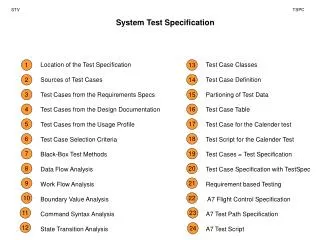
Understanding SoC: A Comprehensive Overview of System on Chip Technology
A System on Chip (SoC) integrates all components of a computer or electronic system into a single chip, including one or more CPU cores, peripheral interfaces, and dedicated hardware blocks. This overview discusses the broader implications of SoCs, differentiating them from ASICs and FPGAs, and highlights the design considerations necessary for modern semiconductor solutions. Emphasis is placed on the innovative design flow and the contemporary relevance of SoCs in optimizing performance, power efficiency, and form-factor in the age of complex electronic systems.

Understanding SoC: A Comprehensive Overview of System on Chip Technology
E N D
Presentation Transcript
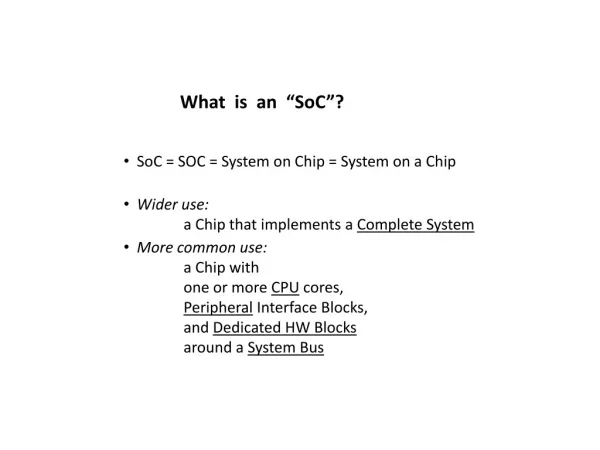
What is an “SoC”? • SoC = SOC = System on Chip = System on a Chip • Wider use: a Chip that implements a Complete System • More common use: a Chip with one or more CPU cores,Peripheral Interface Blocks, and Dedicated HW Blocks around a System Bus
What is ASIC, FPGA, SoC? ASAAS ASAAS ASAAS ASIC FPGA SoC
Individual Gates and MemoryPre-designed All Layout except WiresPre-designed LayoutNot Pre-designed Whole ChipPre-designed Full-custom ASIC Gate-array(Structured ASIC) FPGA SoC
Inside an FPGA CLB: Configurable Logic Block
From a Designer’s Perspective • ASIC, FPGA, SoC: all the same from a designer’s point of view • We are in the SoC age => • Shop for IP blocks (IP block = Library block) • Integrate them with each other and your design
What is ASIC? • IC • Full-custom IC • IC = SP or ASSP • SP = Standard Product = Memory chip, Processor • ASSP = Application Specific Standard Product = USB interface chip for ex. • ASIC => Think of Vestel or Cisco – an equipment=box=system maker that buys ICs (SP or ASSP) puts them on a PCB. They sometimes need extra logic => hence ASIC (Application Specific Integrated Circuit)
Contemporary (wider)meaning of ASIC • Previous slide described the original (narrow) meaning of ASIC (how the word ASIC came about) • Such chips required quick methods for design because: • constraints in design time • constraints in design personnel • designs were not so aggressive • This resulted in what we call: ASIC Design Flow • Hence: an “ASIC Designer” doing “ASIC Design” may be working on an SP done in ASIC Design Flow as opposed to Full-Custom Flow.
Why/when design your own chip or customize an SoC? As opposed to taking a CPU and writing code that runs on it • BECAUSE: • CPU solution is not fast enough (FPGA is slower but offers more parallelism) • CPU is too expensive • CPU sucks too much power • CPU cannot meet the exact I/O timing requirements (no later no earlier) • CPU does not have the right number and mix of I/O pins • Form-factor: CPU is too big and/or requires a heat/sink, fan, and/or chip-set
Top Semi Companies (2011) Fabless semi Intel (USA): $50B Samsung (Korea): $29B/$260B+ TSMC (Taiwan): $15B TI (USA): $14B Toshiba (Japan): $13B/$80B Renesas (Japan): $11B Qualcomm (USA): $10B STMicro (Fr-Ita): $10B Hynix (Korea): $9B Micron (USA): $7B Broadcom (USA): $7B AMD (USA): $6B Infineon (Germany): $5B Sony (Japan): $5B/$90B Freescale (USA): $4B Elpida (Japan): $4B NXP (Holland): $4B UMC (Taiwan): $4B NVIDIA (USA): $4B Globalfoundries (USA): $4B FPGA market size $5B Fab = Foundry
Top FPGA (=PLD=CPLD) Companies(all with HQs in the USA) Xilinx: 49% Altera: 40% Lattice: 6% Microsemi (was Actel): 4% Quicklogic: 1%
ASIC Implementation Flow SW tools = $100K - $1M 3-12 months ASIC Design ~ 2 months Fabrication NRE = $100K - $4M ~ 1 month Package/Test ~ 1 month Validation
ASIC Design Flow spec(behav. code) Back-End Verification(Timing, GateSim,Formal, DRC, LVS) Front-End Design Front-End Verification Specification & Arch. Back-End Design Synthesis/Timing HDL RTL HDL RTL HDL gates Layout in GDSII
ASIC Design Tool-set Editor Back-End Verification(Timing, GateSim,Formal, DRC, LVS) Front-End Design Front-End Verification Back-End Design Synthesis/Timing HDL RTL Simulator SW Stdcell Library HDL RTL Synthesis SW HDL gates Layout in GDSII Physical design, verif., DFT/ATPG SWs
Top EDA Companies(all with HQs in the USA) • Synopsys: $1500M • Mentor Graphics: $900M • Cadence: $850M • Other: 27% • (Above are my 2010 estimates. • Total market size: $4.5B)
FPGA Design Flow spec(behav. code) Back-End Verification(Timing, GateSim,Formal, DRC, LVS) Front-End Design Front-End Verification Specification & Arch. HDL RTL HDL RTL Synthesis,Back-end,Timing Bitfile
FPGA DesignTool-set for Xilinx Front-End Design Front-End Verification HDL RTL Xilinx ISEEditor, Simulator, SynthesisAll in one IDE HDL RTL Synthesis,Back-end,Timing Bitfile
You hardly need anything you learned in your Logic coursein Modern (HDL and Synthesis based) Digital Designbecause: • We write code • We don’t design circuits • At least no gate-level circuits • We don’t care about theorems in Boolean Algebra • We don’t care about Karnaugh-maps • The synthesis SW (compiler)does the logic minimization for us • The FPGA has 1000s of gates anyway • (OK, in some extreme cases we may need to care) • Before we care about area minimizationwe need to care about meeting timing
What does RTL mean in the first place? RTL = RT-Level = Register Transfer Level
What is RT-Level digital (logic) design? Everything is a STATE MACHINE! Your (RTL) code describes the logic cloud storedVars Cloud of Logic(Combinational) more Flops storedVars_next Inputs Flop Outputs
INCREMENTER clk
0 0 0 0 INCREMENTER 0 0 1 0 clk time
0 0 0 0 INCREMENTER 0 0 1 1 clk time
0 0 0 0 INCREMENTER 1 0 0 1 clk time
0 0 0 0 INCREMENTER 1 1 0 0 clk time
0 0 0 0 INCREMENTER 1 1 1 0 clk time
0 0 0 0 INCREMENTER 1 1 1 1 clk time
0 0 1 0 INCREMENTER 0 1 0 1 clk time
Key points in this programming paradigm: • What are we programming? • How will we program? (Any guidelines?) • What is a “flop” by the way?
Flop: What is it? Edge-Triggered D-Type Flip Flop= D-Type Flip Flop= Flip-Flop = Flop Edge-Triggered Flip-Flop as opposed to: Level-Sensitive Transparent Latch = Latch
Flop: explained with WAVEFORMS posedge posedge posedge posedge clk D Q D clk Q Flop = 1-bit DigiCam
2 Flops back to back = Shift Register clk Q1 D Q2 D Q1 clk Q2
How a FLOP behaves (shown with a SHIFT REGISTER) t = before posedge clk flop1 flop2 1 0 0 1 1 1 0 1
How a FLOP behaves (shown with a SHIFT REGISTER) t = posedge clk flop1 flop2 1 1 0 0 1 1 0 1
How a FLOP behaves (shown with a SHIFT REGISTER) C2Q delay like good cholestrol t = posedge clk + C2Q delay flop1 flop2 1 1 1 0 0 1 1 0
SWITCH = LATCH Latch = Transparent Latch clk clk (= enable) D Q