Download
1 / 41
410 likes | 444 Vues
Explore the memory and peripheral busses in microprocessor-based systems, including concepts like power-on reset, vector tables, memory access in C, and the APB bus.

E N D
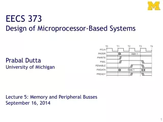
EECS 373 Design of Microprocessor-Based Systems Prabal Dutta University of Michigan Lecture 5: Memory and Peripheral Busses September 16, 2014
Announcements • Homework #2 • Where was I last week? • VLCS’14 • MobiCom’14 • HotWireless’14
Emerging Retail Environment: A Walled Garden • Often have line-of-sight to lighting • Groceries • Drugstores • Megastores • Hardware stores • Enterprise settings • Lots of overhead lighting in retail • Retailers deploying LED lighting • Customers using phones in stores • Surf, Scan, Share • Customers installing retailer apps • Maps, Barcodes, Deals, Shopping
Visible Light Communications and Positioning 01100101000 Idle TX <66> Illuminate TX packet Smart Phone LED Luminaire Captured using a rolling shutter f4 S4 f3 S3 f2 S2 S4 f1 Image processing extracts beacon locations and frequencies S3 S1 S2 Compute S1 Minimize
Outline • Announcements • Review • ARM AHB-Lite
What happens after a power-on-reset (POR)? • On the ARM Cortex-M3 • SP and PC are loaded from the code (.text) segment • Initial stack pointer • LOC: 0x00000000 • POR: SP mem(0x00000000) • Interrupt vector table • Initial base: 0x00000004 • Vector table is relocatable • Entries: 32-bit values • Each entry is an address • Entry #1: reset vector • LOC: 0x0000004 • POR: PC mem(0x00000004) • Execution begins .equ STACK_TOP, 0x20000800 .text .syntax unified .thumb .global _start .type start, %function _start: .word STACK_TOP, start start: movs r0, #10 ...
Accessing memory locations from C #define SYSREG_SOFT_RST_CR 0xE0042030 uint32_t *reg = (uint32_t *)(SYSREG_SOFT_RST_CR); main () { *reg |= 0x00004000; // Reset GPIO hardware *reg &= ~(0x00004000); } Memory has an address and value Can equate a pointer to desired address Can set/get de-referenced value to change memory
Some useful C keywords • const • Makes variable value or pointer parameter unmodifiable • const foo = 32; • register • Tells compiler to locate variables in a CPU register if possible • register int x; • static • Preserve variable value after its scope ends • Does not go on the stack • static int x; • volatile • Opposite of const • Can be changed in the background • volatile int I;
What happens when this“instruction” executes? #include <stdio.h> #include <inttypes.h> #define REG_FOO 0x40000140 main () { uint32_t *reg = (uint32_t *)(REG_FOO); *reg += 3; printf(“0x%x\n”, *reg); // Prints out new value }
“*reg += 3” is turned into a ld, add, str sequence • Load instruction • A bus read operation commences • The CPU drives the address “reg” onto the address bus • The CPU indicated a read operation is in process (e.g. R/W#) • Some “handshaking” occurs • The target drives the contents of “reg” onto the data lines • The contents of “reg” is loaded into a CPU register (e.g. r0) • Add instruction • An immediate add (e.g. add r0, #3) adds three to this value • Store instruction • A bus write operation commences • The CPU drives the address “reg” onto the address bus • The CPU indicated a write operation is in process (e.g. R/W#) • Some “handshaking” occurs • The CPU drives the contents of “r0” onto the data lines • The target stores the data value into address “reg”
Modern embedded systems have multiple busses Atmel SAM3U Expanded 373 focus Historical 373 focus
Why have so many busses? • Many designs considerations • Master vs Slave • Internal vs External • Bridged vs Flat • Memory vs Peripheral • Synchronous vs Asynchronous • High-speed vs low-speed • Serial vs Parallel • Single master vs multi master • Single layer vs multi layer • Multiplexed A/D vs demultiplexed A/D • Discussion: what are some of the tradeoffs?
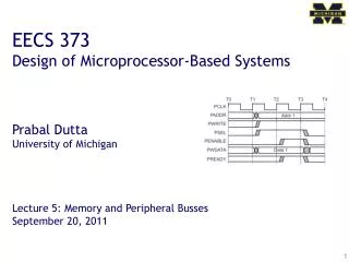
APB • IDLE • Default APB state • SETUP • When transfer required • PSELx is asserted • Only one cycle • ACCESS • PENABLE is asserted • Addr, write, select, and write data remain stable • Stay if PREADY = L • Goto IDLE if PREADY = H and no more data • Goto SETUP is PREADY = H and more data pending Setup phase begins with this rising edge Setup Phase Access Phase
APB signal definitions • PCLK: the bus clock source (rising-edge triggered) • PRESETn: the bus (and typically system) reset signal (active low) • PADDR: the APB address bus (can be up to 32-bits wide) • PSELx: the select line for each slave device • PENABLE: indicates the 2nd and subsequent cycles of an APB xfer • PWRITE: indicates transfer direction (Write=H, Read=L) • PWDATA: the write data bus (can be up to 32-bits wide) • PREADY: used to extend a transfer • PRDATA: the read data bus (can be up to 32-bits wide) • PSLVERR: indicates a transfer error (OKAY=L, ERROR=H)
Let’s say we want a device that provides data froma switch on a read to any address it is assigned. (so returns a 0 or 1) PWRITE PENABLE PSEL PADDR[7:0] PCLK PREADY PRDATA[32:0] Mr. Switch
Device provides data from switch A if address 0x00001000 is read from. B if address 0x00001004is read from PWRITE PENABLE PSEL PADDR[7:0] PCLK PREADY PRDATA[32:0] Mr. Switch Mrs. Switch
32-bit Reg D[31:0] Q[31:0] EN C All reads read from register, all writes write… PWDATA[31:0] PWRITE PENABLE PSEL PADDR[7:0] PCLK PREADY PREADY PRDATA[32:0] We are assuming APB only gets lowest 8 bits of address here…
Outline • Announcements • Review • ARM AHB-Lite
Advanced Microcontroller Bus Architecture (AMBA)- Advanced High-performance Bus (AHB)- Advanced Peripheral Bus (APB) AHB APB Low power Latched address/control Simple interface Suitable of many peripherals • High performance • Pipelined operation • Burst transfers • Multiple bus masters • Split transactions
AHB-Lite supports single bus masterand provides high-bandwidth operation • Burst transfers • Single clock-edge operation • Non-tri-state implementation • Configurable bus width
AHB-Lite bus master/slave interface • Global signals • HCLK • HRESETn • Master out/slave in • HADDR (address) • HWDATA (write data) • Control • HWRITE • HSIZE • HBURST • HPROT • HTRANS • HMASTLOCK • Slave out/master in • HRDATA (read data) • HREADY • HRESP
AHB-Lite signal definitions • Global signals • HCLK: the bus clock source (rising-edge triggered) • HRESETn: the bus (and system) reset signal (active low) • Master out/slave in • HADDR[31:0]: the 32-bit system address bus • HWDATA[31:0]: the system write data bus • Control • HWRITE: indicates transfer direction (Write=1, Read=0) • HSIZE[2:0]: indicates size of transfer (byte, halfword, or word) • HBURST[2:0]: indicates single or burst transfer (1, 4, 8, 16 beats) • HPROT[3:0]: provides protection information (e.g. I or D; user or handler) • HTRANS: indicates current transfer type (e.g. idle, busy, nonseq, seq) • HMASTLOCK: indicates a locked (atomic) transfer sequence • Slave out/master in • HRDATA[31:0]: the slave read data bus • HREADY: indicates previous transfer is complete • HRESP: the transfer response (OKAY=0, ERROR=1)
Key to timing diagram conventions • Timing diagrams • Clock • Stable values • Transitions • High-impedance • Signal conventions • Lower case ‘n’ denote active low (e.g. RESETn) • Prefix ‘H’ denotes AHB • Prefix ‘P’ denotes APB
Basic read and write transfers with no wait states Pipelined Address & Data Transfer
Read transfer with two wait states Valid data produced Two wait states added by slave by asserting HREADY low
Write transfer with one wait state Valid data held stable One wait state added by slave by asserting HREADY low
Wait states extend the address phase of next transfer Address stage of the next transfer is also extended One wait state added by slave by asserting HREADY low
Transfers can be of four types (HTRANS[1:0]) • IDLE (b00) • No data transfer is required • Slave must OKAY w/o waiting • Slave must ignore IDLE • BUSY (b01) • Insert idle cycles in a burst • Burst will continue afterward • Address/control reflects next transfer in burst • Slave must OKAY w/o waiting • Slave must ignore BUSY • NONSEQ (b10) • Indicates single transfer or first transfer of a burst • Address/control unrelated to prior transfers • SEQ (b11) • Remaining transfers in a burst • Addr = prior addr + transfer size
A four beat burst with master busy and slave wait Master busy indicated by HTRANS[1:0] One wait state added by slave by asserting HREADY low
Controlling the size (width) of a transfer • HSIZE[2:0] encodes the size • The cannot exceed the data bus width (e.g. 32-bits) • HSIZE + HBURST is determines wrapping boundary for wrapping bursts • HSIZE must remain constant throughout a burst transfer
Controlling the burst beats (length) of a transfer • Burst of 1, 4, 8, 16, and undef • HBURST[2:0] encodes the type • Incremental burst • Wrapping bursts • 4 beats x 4-byte words wrapping • Wraps at 16 byte boundary • E.g. 0x34, 0x38, 0x3c, 0x30,… • Bursts must not cross 1KB address boundaries
An eight beat incrementing burst(INCR8) using half-word transfers
Multi-master AHB-Lite requires a multi-layer interconnect • AHB-Lite is single-master • Multi-master operation • Must isolate masters • Each master assigned to layer • Interconnect arbitrates slave accesses • Full crossbar switch often unneeded • Slaves 1, 2, 3 are shared • Slaves 4, 5 are local to Master 1
Questions? Comments? Discussion?