Download
1 / 54
540 likes | 572 Vues
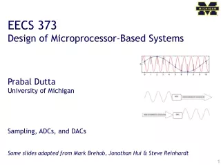
EECS 373 Design of Microprocessor-Based Systems Prabal Dutta University of Michigan AMBA: Advanced Microcontroller Bus Architecture AHB: AMBA High-performance Bus APB: Advanced Peripheral Bus. Slides developed in part by Mark Brehob & Prabal Dutta.

E N D
EECS 373 Design of Microprocessor-Based Systems Prabal Dutta University of Michigan AMBA: Advanced Microcontroller Bus Architecture AHB: AMBA High-performance Bus APB: Advanced Peripheral Bus Slides developed in part by Mark Brehob & Prabal Dutta
Busses: the glue that connects the pieces C Assembly Machine Code Central Processing Unit EECS 370 Software Hardware ISA ldr (read) str (write) bl (int) System Buses AHB/APB Interrupts GPIO/INT Internal & External Memory Timers USART DAC/ADC Internal External EMC SPI DAC I2C ADC Input UART Output Capture Compare Interrupt
Today… MMIO: Memory-Mapped I/O review AMBA: Advanced Microcontroller Bus Architecture APB: Advanced Peripheral Bus AHB: AMBA High-performance Bus
Memory-Mapped I/O (MMIO) • I/O model in which the same address bus/space is used to • Do memory accesses (e.g. to RAM) • Do I/O operations (e.g. to I/O pins or peripheral registers) • Reading and writing memory addresses allows us to • Read peripheral state (e.g. value of an I/O pin or FSM’s DFF) • Issue peripheral commands (e.g. set an I/O pin or FSM’s state) • How? • Memory has an address and value • Can equate a pointer to desired address • Can set/get de-referenced value to change memory • Can control peripheral state in this way
Reading register bits with MMIO #define PBS_REG 0xB0000003 int isBlueButtonPressed() { return (*((uint32_t *)PBS_REG) & 0x00000004) >> 2; } • How? • Let’s say that red, green, and blue pushbuttons are mapped to memory address 0xB0000003 at bits 0, 1, and 2, respectively • When pushed, we will read a ‘1’ from the corresponding bit • When released, we will read a ‘0’ from the corresponding bit Address \ Bit 31 24 23 16 15 8 7 210 0xB0000003 -------- -------- -------- ----- • Must mask (and perhaps shift) to select target bits for reading
Writing register bits with MMIO #define LED_REG 0xB0000004 void setRedLed() { *((uint32_t *)LED_REG) |= 0x1; } void setGreenLed() { *((uint32_t *)LED_REG) |= 0x2; } #define LED_REG 0xB0000004 void clearRedLed() { *((uint32_t *)LED_REG) &= ~(0x00000001); } void clearBlueLed() { *((uint32_t *)LED_REG) &= ~(0x00000004); } • How? • Let’s say that red, green, and blue LEDs are mapped to memory address 0xB0000004 at bits 0, 1, and 2, respectively • Writing a ‘1’ (‘0’) to the corresponding bit turns on (off) the LED Address \ Bit 31 24 23 16 15 8 7 210 0xB0000004 -------- -------- -------- ----- • When updating (set/clear) bits, must preserve remaining contents • Use bitmask to select target bits for manipulation, e.g.
Some useful C keywords • const • Makes variable value or pointer parameter unmodifiable • const foo = 32; • register • Tells compiler to locate variables in a CPU register if possible • register int x; • static • Preserve variable value after its scope ends • Does not go on the stack • static int x; • volatile • Opposite of const • Can be changed in the background • volatile int I;
Today… MMIO: Memory-Mapped I/O review AMBA: Advanced Microcontroller Bus Architecture APB: Advanced Peripheral Bus AHB: AMBA High-performance Bus
Advanced Microcontroller Bus Architecture (AMBA)- Advanced/AMBA High-performance Bus (AHB)- Advanced Peripheral Bus (APB) AHB APB Low power Latched address/control Simple interface Suitable of many peripherals • High performance • Pipelined operation • Burst transfers • Multiple bus masters • Split transactions
Today… MMIO: Memory-Mapped I/O review AMBA: Advanced Microcontroller Bus Architecture APB: Advanced Peripheral Bus AHB: AMBA High-performance Bus
APB: a simple bus that is easy to work with • Low-cost • Low-power • Low-complexity • Low-bandwidth • Non-pipelined • Ideal for peripherals
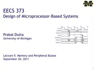
APB bus state machine • IDLE • Default APB state • SETUP • When transfer required • PSELx is asserted • Only one cycle • ACCESS • PENABLE is asserted • Addr, write, select, and write data remain stable • Stay if PREADY = L • Goto IDLE if PREADY = H and no more data • Goto SETUP is PREADY = H and more data pending Setup phase begins with this rising edge Setup Phase Access Phase
APB signal definitions • PCLK: the bus clock source (rising-edge triggered) • PRESETn: the bus (and typically system) reset signal (active low) • PADDR: the APB address bus (can be up to 32-bits wide) • PSELx: the select line for each slave device • PENABLE: indicates the 2nd and subsequent cycles of an APB xfer • PWRITE: indicates transfer direction (Write=H, Read=L) • PWDATA: the write data bus (can be up to 32-bits wide) • PREADY: used to extend a transfer • PRDATA: the read data bus (can be up to 32-bits wide) • PSLVERR: indicates a transfer error (OKAY=L, ERROR=H)
APB bus signals in action • PCLK • Clock • PADDR • Address on bus • PWRITE • 1=Write, 0=Read • PWDATA • Data written to the I/O device. Supplied by the bus master/processor.
APB bus signals • PSEL • Asserted if the current bus transaction is targeted to this device • PENABLE • High during entire transaction other than the first cycle. • PREADY • Driven by target. Similar to our #ACK. Indicates if the target is ready to do transaction.Each target has it’s own PREADY
A write transfer with no wait states Setup phase begins with this rising edge Setup Phase Access Phase
A write transfer with wait states Setup phase begins with this rising edge Setup Phase Wait State Wait State Access Phase
A read transfer with no wait states Setup phase begins with this rising edge Setup Phase Access Phase
A read transfer with wait states Setup phase begins with this rising edge Setup Phase Wait State Wait State Access Phase
Example setup • We will assume we have one bus master “CPU” and two slave devices (D1 and D2) • D1 is mapped to 0x00001000-0x0000100F • D2 is mapped to 0x00001010-0x0000101F
Writes Let’s do some hardware examples!
32-bit Reg D[31:0] Q[31:0] EN C Design a device which writes to a register wheneverany address in its range is written What if we want to have the LSB of this register control an LED? PWDATA[31:0] PWRITE PENABLE PSEL PADDR[7:0] PCLK PREADY LED We are assuming APB only gets lowest 8 bits of address here…
32-bit Reg A D[31:0] Q[31:0] EN C 32-bit Reg B D[31:0] Q[31:0] EN C Reg A should be written at address 0x00001000Reg B should be written at address 0x00001004 PWDATA[31:0] PWRITE PENABLE PSEL PADDR[7:0] PCLK PREADY We are assuming APB only gets lowest 8 bits of address here…
Reads… The key thing here is that each slave device has its own read data (PRDATA) bus! Recall that “R” is from the initiator’s viewpoint—the device drives data when read.
Let’s say we want a device that provides data froma switch on a read to any address it is assigned. (so returns a 0 or 1) PWRITE PENABLE PSEL PADDR[7:0] PCLK PREADY PRDATA[32:0] Mr. Switch
Device provides data from switch A if address 0x00001000 is read from. B if address 0x00001004is read from PWRITE PENABLE PSEL PADDR[7:0] PCLK PREADY PRDATA[31:0] Mr. Switch Mrs. Switch
32-bit Reg D[31:0] Q[31:0] EN C All reads read from register, all writes write… PWDATA[31:0] PWRITE PENABLE PSEL PADDR[7:0] PCLK PREADY PREADY PRDATA[31:0] We are assuming APB only gets lowest 8 bits of address here…
Things left out… • There is another signal, PSLVERR (APB Slave Error) which we can drive high if things go bad. • We’ll just tie that to 0. • PRESETn • Active low system reset signal • (needed for stateful peripherals) • Note that we are assuming that our device need not stall. • We could stall if needed. • I can’t find a limit on how long, but I suspect at some point the processor would generate an error.
Actel/Microsemi implementation of CoreAPB3 • ARM APB spec is silent about sharing signals • PSEL, PREADY, PRDATA are shared • Hence, every peripheral needs its own decode logic…which is cumbersome • Actel CoreAPB3 (and other) module(s) help • Allocates per-slave signals • PSEL, PREADY, PRDATA, PSLVERR broken out • CoreAPB3 supports 16 slaves • Performs address decoding for PSEL • De-multiplexes PSEL signal • Multiplexes PREADY, PRDATA, PSLVERR
Today… MMIO: Memory-Mapped I/O review AMBA: Advanced Microcontroller Bus Architecture APB: Advanced Peripheral Bus AHB: AMBA High-performance Bus
AHB-Lite supports single bus masterand provides high-bandwidth operation • Burst transfers • Single clock-edge operation • Non-tri-state implementation • Configurable bus width
AHB-Lite bus master/slave interface • Global signals • HCLK • HRESETn • Master out/slave in • HADDR (address) • HWDATA (write data) • Control • HWRITE • HSIZE • HBURST • HPROT • HTRANS • HMASTLOCK • Slave out/master in • HRDATA (read data) • HREADY • HRESP
AHB-Lite signal definitions • Global signals • HCLK: the bus clock source (rising-edge triggered) • HRESETn: the bus (and system) reset signal (active low) • Master out/slave in • HADDR[31:0]: the 32-bit system address bus • HWDATA[31:0]: the system write data bus • Control • HWRITE: indicates transfer direction (Write=1, Read=0) • HSIZE[2:0]: indicates size of transfer (byte, halfword, or word) • HBURST[2:0]: indicates single or burst transfer (1, 4, 8, 16 beats) • HPROT[3:0]: provides protection information (e.g. I or D; user or handler) • HTRANS: indicates current transfer type (e.g. idle, busy, nonseq, seq) • HMASTLOCK: indicates a locked (atomic) transfer sequence • Slave out/master in • HRDATA[31:0]: the slave read data bus • HREADY: indicates previous transfer is complete • HRESP: the transfer response (OKAY=0, ERROR=1)
Key to timing diagram conventions • Timing diagrams • Clock • Stable values • Transitions • High-impedance • Signal conventions • Lower case ‘n’ denote active low (e.g. RESETn) • Prefix ‘H’ denotes AHB • Prefix ‘P’ denotes APB
Basic read and write transfers with no wait states Pipelined Address & Data Transfer
Read transfer with two wait states Valid data produced Two wait states added by slave by asserting HREADY low
Write transfer with one wait state Valid data held stable One wait state added by slave by asserting HREADY low
Wait states extend the address phase of next transfer Address stage of the next transfer is also extended One wait state added by slave by asserting HREADY low
Today… MMIO: Memory-Mapped I/O review AMBA: Advanced Microcontroller Bus Architecture APB: Advanced Peripheral Bus AHB: AMBA High-performance Bus - Low-level details included for completeness - But we’ll skip most of these details
Transfers can be of four types (HTRANS[1:0]) • IDLE (b00) • No data transfer is required • Slave must OKAY w/o waiting • Slave must ignore IDLE • BUSY (b01) • Insert idle cycles in a burst • Burst will continue afterward • Address/control reflects next transfer in burst • Slave must OKAY w/o waiting • Slave must ignore BUSY • NONSEQ (b10) • Indicates single transfer or first transfer of a burst • Address/control unrelated to prior transfers • SEQ (b11) • Remaining transfers in a burst • Addr = prior addr + transfer size
A four beat burst with master busy and slave wait Master busy indicated by HTRANS[1:0] One wait state added by slave by asserting HREADY low
Controlling the size (width) of a transfer • HSIZE[2:0] encodes the size • The cannot exceed the data bus width (e.g. 32-bits) • HSIZE + HBURST is determines wrapping boundary for wrapping bursts • HSIZE must remain constant throughout a burst transfer
Controlling the burst beats (length) of a transfer • Burst of 1, 4, 8, 16, and undef • HBURST[2:0] encodes the type • Incremental burst • Wrapping bursts • 4 beats x 4-byte words wrapping • Wraps at 16 byte boundary • E.g. 0x34, 0x38, 0x3c, 0x30,… • Bursts must not cross 1KB address boundaries