Embedded System Testing & Debugging Course Overview and Schedule
This course covers vital aspects of embedded system testing and debugging, with key dates including project due dates, a final exam, and crucial report and presentation slots. Topics include A/D conversion, real-time constraints, embedded operating systems, and control systems. The course emphasizes the importance of thorough testing in hardware and software environments, outlines techniques such as JTAG and BIST, and discusses unique challenges in embedded system testing. Prepare with reviewed slides and notes, and think critically like a professor to deepen your understanding.

Embedded System Testing & Debugging Course Overview and Schedule
E N D
Presentation Transcript
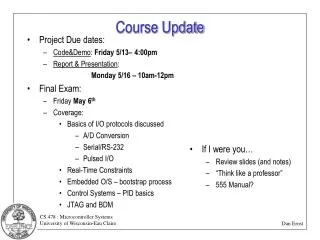
Course Update • Project Due dates: • Code&Demo: Friday5/13– 4:00pm • Report & Presentation: Monday5/16 – 10am-12pm • Final Exam: • Friday May 6th • Coverage: • Basics of I/O protocols discussed • A/D Conversion • Serial/RS-232 • Pulsed I/O • Real-Time Constraints • Embedded O/S – bootstrap process • Control Systems – PID basics • JTAG and BDM • If I were you… • Review slides (and notes) • “Think like a professor” • 555 Manual?
Testing • Just like in software, embedded systems need to be tested and debugged • However, in these systems, testing includes multiple facets! • Chip/component verification • Circuit boards / External devices • Software, including system startup and configuration • Hardware has a much higher penalty for correctness mistakes • You can’t “patch” hardware • Recalls are expensive (on several levels) Q: How many Pentium designers does it take to screw in a light bulb? A: 1.99904274017, but that's close enough for non-technical people.
Chip Testing • Post-production testing of a chip (in a basic test harness) became a very difficult (and expensive) part of a chip’s production • Involves the design of large test suites to send through the pins • Involves very expensive test harnesses to be able to run these quickly • Modern systems often use Built-In Self Test (BIST) blocks within the chip that will run a number of internal tests automatically • Example: RAM test in your PC BIOS
PCB Testing • Older systems used the “bed of nails” technique for testing PCB connections to make sure they were correct. • Probe the PCB wires with test pins, whichwere then toggled for tests • When pin densities got very tight,this became too difficult (and expensive)
JTAG • Mid/Late 80s: a group of companies banded together to define standards for including hardware to do this testing • Joint Test Access Group (JTAG) • 1990: IEEE made it standard 1149.1 • IEEE Standard Test Access Port and Boundary Scan Architecture • Boundary Scan • Chip can be put into a “test mode”,where built-in testing blocks takeover the use of the pins
JTAG • The TAP controller runs the show for the internal logic. • 4 pins control operation: • 2 Serial Data pins • TDI (Test Data In) • TDO (Test Data Out) • TCK (Test Clock) • TMS (Test Mode Select) • Required Instructions: • EXTEST • SAMPLE/PRELOAD • BYPASS • All individual cells together form the “Boundary Scan Register” • MPC555: 346 bits
Software Testing • Testing embedded/controller software has a few extra factors to it: • Program often maintained in a ROM • Often very interrupt driven • Often reliant on operation of peripheral devices • This means that, without having the actual hardware at your disposal, testing software can be next to impossible • Most embedded systems don’t have a standard interface (keyboard/mouse/VGA) • Need a way to get debugging information to a more developer-friendly platform
Background Debug Mode (BDM) • Most embedded processor manufacturers now include a “Development Port” of some kind to support remote debugging • Observe contents of registers and memories • Hardware breakpoints • Single-step • Ref: MPC555 Manual, Section 21
Development Port Operation • 3 pins: • DSCK • DSDI • DSDO • When “debug mode” is entered, the processor stops fetching instructions from memory • Instructions are entered through the DPIR (instruction register)
Pausing Execution • Execution can be stopped a number of ways with this setup: • Setting breakpoints • Implemented by a set of comparison registers • Catching interrupts • Debug Enable Register (DER) sets which ones should flag a break • External input • Click the “stop button” in CodeWarrior • On a pause, the FRZ (Freeze) signal is also enabled • Pauses all counters in peripherals, if set up that way