Lecture #7 EGR 277 – Digital Logic
120 likes | 403 Vues
Lecture #7 EGR 277 – Digital Logic. Reading Assignment: Chapter 4 in Digital Design, 3 rd Edition by Mano. Chapter 4 – Combinational Logic Circuits A) Using gates (with the Design Procedure covered shortly) B) Using commercially-available MSI and LSI devices

Lecture #7 EGR 277 – Digital Logic
E N D
Presentation Transcript
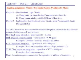
Lecture #7 EGR 277 – Digital Logic Reading Assignment: Chapter 4 in Digital Design, 3rd Edition by Mano • Chapter 4 – Combinational Logic Circuits • A) Using gates (with the Design Procedure covered shortly) • B) Using commercially-available MSI and LSI devices • Chapter 5 – Implementing Combinational Logic Circuits using Programmable Logic • Devices (PLD’s) • The terms below have become somewhat dated as integrated circuits have become more complex, but they are still used at times: • SSI: Small-scale integration - equivalent of 1 - 9 gates • MSI: Medium-scale integration - equivalent of 10 - 99 gates • Examples: Decoders, encoders, multiplexers, adders • LSI: Large-scale integration - equivalent of 100 - 999 gates • Examples: Small memory chips, arithmetic logic units (ALU’s) • VLSI: Very large-scale integration - equivalent of 1000 - 9999 gates • Examples: Small microprocessors • Note: Current microprocessors contain the equivalent of millions of transistors.
Logic N inputs M outputs Gates Lecture #7 EGR 277 – Digital Logic Design Procedure for Combinational Logic Circuits In general, we might want to design a combinational logic circuit with N inputs and M outputs, as shown below. Design Procedure: 1. State the problem 2. Determine the required inputs and outputs 3. Assign variables to the inputs and outputs 4. Derive the truth table 5. Simplify the output expressions 6. Implement the expressions with logic gates
Lecture #7 EGR 277 – Digital Logic Example: Design a prime number indicator that will detect prime numbers with up to 4 bits.
Lecture #7 EGR 277 – Digital Logic • Example: Various types of code converters can be designed, including: • BCD to excess-3 (try this one in class) • ASCII to EBCDIC • Binary to 2’s complement • Excess-3 to reflected • BCD to 9’s complement
Lecture #7 EGR 277 – Digital Logic Example: Half-adder – adds 2 bits with no carry in and one carry out
Lecture #7 EGR 277 – Digital Logic • Example: Full-adder – adds 2 bits with one carry in and one carry out • Illustrate the SOP implementation • Illustrate the XOR implementation • Show how a full adder can be constructed using two half adders
Lecture #7 EGR 277 – Digital Logic • Adders: (continued) Discuss each of the following: • 4-bit adder using 4 full adders • 7483 4-bit adder (explain “look-ahead carry” circuit) • Handout: 7483 data sheet
Lecture #7 EGR 277 – Digital Logic Combinational Logic Using MSI and LSI devices We have the capability to design our own combinational logic circuits, but circuits of common interest are probably available commercially. Commercial devices can perform complex functions using perhaps a single IC, thus saving space. They are typically faster that equivalent circuits that we might build using discrete logic gates. It might be a good idea to browse through a Logic Data Book to see what is available. A few devices are listed below. Assortment of commercially available combinational logic devices
Lecture #7 EGR 277 – Digital Logic Decoders An N-bit decoder has 2N outputs, only one of which may be activated at a given time. If the device is active-HIGH , then only one output may be HIGH at any time. If the device is active-LOW , then only one output may be LOW at any time. Example: A 3-bit decoder might also be called a 3-line-to-8-line decoder or a 3x8 decoder. The block diagram is shown below: • Discuss: • basic operation • the truth table • the design of the decoder circuit.
Lecture #7 EGR 277 – Digital Logic Active-LOW versus Active-HIGH decoders Enable lines – essentially act as ON/OFF switches Example: Show the truth table and block diagram for an active-LOW 2x4 decoder with an enable line, E.
Lecture #7 EGR 277 – Digital Logic Implementing Boolean functions using decoders Note that the decoder outputs for active-HIGH decoders are simply minterms, so F = (minterms) = (active-HIGH decoder outputs) Example: Implement f(A,B,C) = (0, 3, 5, 6) using a 3 x 8 decoder with active-HIGH outputs Note that the decoder outputs for active-LOW decoders are simply maxterms, so F = (maxterms) = (active-LOW decoder outputs) Example: Implement f(A,B,C) = (0, 3, 5, 6) using a 3 x 8 decoder with active-LOW outputs
Lecture #7 EGR 277 – Digital Logic Decoder IC’s Handout: 74155 (dual 2x4 decoder/single 3x8 decoder) Note: The 74156 is similar to the 74155 except that it has open-collector outputs instead of totem-pole outputs (discuss the advantage of this). Show how to connect the 74155 as a 2x4 decoder and also as a 3x8 decoder. Show how to use two 74155’s to form a 4x16 decoder.


