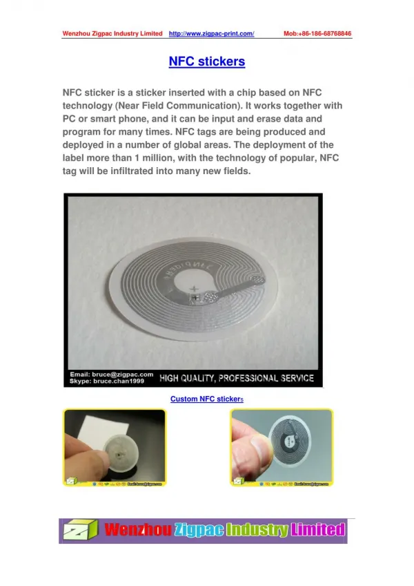
NCTU NFC
NCTU NFC. 高解析度場發射掃描電子顯微鏡暨能量散佈分析儀 Scanning Electron Microscope (S-4700I). Tool expert: Prof. Shun-Tun Yen Technician : Ms. Lien-Chu Chen. Tool name. Chinese name : 高解析度場發射掃描式電子顯微鏡 暨 能量散佈分析儀 English name : High-Resolution Scanning Electron Microscope
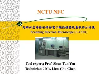

NCTU NFC
E N D
Presentation Transcript
NCTU NFC 高解析度場發射掃描電子顯微鏡暨能量散佈分析儀 Scanning Electron Microscope (S-4700I) Tool expert: Prof. Shun-Tun Yen Technician:Ms. Lien-Chu Chen
Tool name • Chinese name: 高解析度場發射掃描式電子顯微鏡 暨 能量散佈分析儀 • English name: High-Resolution Scanning Electron Microscope & Energy Dispersive Spectrometer • Acronym: SEM & EDS
Tool info • manufacturer:Hitachi • model:S-4700I • Date of purchase:May 1st, 1999.
Features • SEM: High-resolution inspection of devices, thin films, and cross-sections. • EDS: Energy-dispersive spectroscopic analysis of material or contamination composition on a desired spot.
Tool spec • E-gun source:Cold cathodic E-gun • Operation voltage:0.5kV~30kV • Sample size:25mm diameter x 25mm(t) • Working distance:current setting at 12mm • resolution:1.5nm (at 15kV) or 2.5nm (at 1kV) • Highest mag: 500K(depending on the sample) • Resolution of secondary electrons:1.5nm(below 15kV) • EDS could provide qualitative/quantitative atomic (B5~U92) and elemental distribution analysis across the whole energy spectrum .
Principles of SEM (Scanning Electron Microscope) • Tool introduction • E-gun: electron source • Electromagnetic lens: for altering electron path direction • Optical focus system • Principles • Electron migration path • Interactions between electrons and matters • Vacuum necessity and specimen chamber structure.
Vacuum system Good vacuum is prerequisite for obtaining high quality images in SEM The vacuum is maintained by the following pumps : • Electron chamber and electromagnetic lens: 3ion pumps • S.C.-Specimen Chamber: cycled-water chilled diffusion pump and rough pumping by a rotary pump • S.E.C.- Specimen Exchange Chamber: Rotary pump
Operation procedures • Procedures:SEM basic SOP( please click)
Tips • Good sample conductivity: The sample should be highly conductive to ensure sufficient detection of secondary electrons and clear images. Pt or Au capping can help improve the conductivity. However, too thin the capping does not help a lot and too thick of it might cover the inspected area. For less conductive samples such as Si or SiO2, it is recommended to attach the carbon tape on the sample front side after Au deposition. This way, electrons are attracted toward the stage and only a slit is available for secondary electrons.
Tips • Avoid vibration: For high-mag inspection, make sure the sample is firmly attachedand the stage is well fastened. Stage lock feature can be enabled to reduce the vibration caused by external factors. (Once stage lock is enabled, tilt cannot be adjusted)
Tips • Vacuum:the lower the better • Accelerating voltage: higher voltage can lead to better images. The maximum voltage a sample can withstand depends on its own properties. Too high the voltage might damage the sample and result in pollutant generation. • Discretion, attention, and patience are highly appreciated.
Gold particles with 10K mag SEMPictures—taken by Ms. Yue-Ting Chen mag 500nm for each spacing
mag SEMPictures—taken by Ms. Yue-Ting Chen • Surface of gold particles is clear with 150 K mag 30nm for each spacing
mag SEMPictures—taken by Ms. Yue-Ting Chen • Surface of gold particles with 250 K mag 20nm for each spacing
mag SEMPictures—taken by Ms. Yue-Ting Chen • Surface of gold particles with 300 K mag 10nm for each spacing
mag SEMPictures—taken by Ms. Yue-Ting Chen • Surface of gold particles with 400 K mag 10nm for each spacing
mag SEMPictures—taken by Ms. Yue-Ting Chen • Surface of gold particles with 450 K mag 10nm for each spacing
10nm for each spacing mag mag SEMPictures—taken by Ms. Yue-Ting Chen • Surface of gold particles with 500 K mag 10nm for each spacing
SEMPictures—taken by Ms. Yue-Ting Chen The following pictures are taken by students from various affiliations. Through SEM, we can share our own skills and excellent pictures.
SEMPictures—taken by a student Carbon nano tube
SEMPictures—taken by a student Zno nanowire
SEMPictures—taken by a student MOSFET device
SEMPictures—taken by a student High-K material
SEMPictures—taken by a student Material for high-frequency devices
SEMPictures—taken by a student High-speed device
SEMPictures—taken by a student SiO2nanoparticle-fixing substrate
SEMPictures—taken by a student polymer micelles
SEMPictures—taken by a student Carbon nano tube
SEMPictures—taken by a student CeO nano cube
SEMPictures—taken by a student photonic crystal
SEMPictures—taken by a student Nanoscale linewidth
SEMPictures—taken by a student Surface analysis
SEMPictures—taken by a student Surface analysis of Ti
SEMPictures—taken by a student GaN surface roughening for blue light LED
SEMPictures—taken by a student Oxide-based nanowire
SEMPictures—taken by a student Nylon film
SEMPictures—taken by a student Blocking layer deposited via PECVD on Pet film
Conclusion Please cherish this multi-functional SEM !!