Power Dissipation in Nanoelectronics
Power Dissipation in Nanoelectronics. R. Pecora, S. Belavadi , D. Estrada Pop Research Group ECE Dept., University of Illinois, Urbana, IL 61801. Why is this Important?.

Power Dissipation in Nanoelectronics
E N D
Presentation Transcript
Power Dissipation in Nanoelectronics R. Pecora, S. Belavadi, D. Estrada Pop Research Group ECE Dept., University of Illinois, Urbana, IL 61801
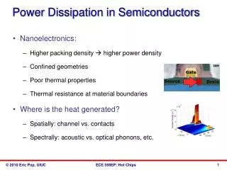
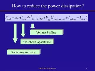
Why is this Important? • Modern electronics such as CPUs generate substantial amounts of heat. This heat has to go somewhere, and it severely limits further improvements to devices. • Lots of power is used up in memory, while PCM can use less energy for more memory density(Making your tiny Ipod nano even smaller)
CNT – Carbon Nano Tubes • Allotropes of carbon and are 1D hexagonally arranged C atoms. • Properties: High thermal conductivity, electrical conductivity, tensile strength… • DNA( diameter~ 2.5nm) • SWCNT( diameter~ 1.7nm)
Bottom-Up Approach • Target the source of the heat generation, instead of looking into bigger and better cooling. • Graphene: Graphite on the nano level • CNTFET(Carbon Nano Tube Field Effect Transistor): Smaller and less resistive than traditional Higher Transistor Density! • PCM(Phase Change Material): Material that changes phase depending on heating method and temperature. Heater Random CNT Film Sensor Sensor 50µm
V = 0 V S DS I D SiO 2 Current Projects • Phase Change Memory: Heat GST(Germanium Antimony Tellurium) to make a binary 1 or 0. • Thermal Properties of CNTs and Graphene: Establish reliable thermal data and models. • Transistor Reliability: Test limits on CNT Transistors; breakdown and hysteresis. Carbon NanotubeField Effect Transistor V GS ≈ ≈
Calibrating The Infrascope II • Helped MNTL Staff setup and calibrate an Infrascope II Infrared Microscope. LN2 jacket for IR detector cooling 1X, 5X, and 15X objectives Vibration Isolation Table PC for data acquisition
Thermal Imaging With Scope • Took both .jpg(for pretty colors) and .txt(for analysis) of several different devices and temperatures. Put current through device to observe heating effect. Early image of heating device [°C]
FET – Field Effect Transistors • Voltage controlled devices
V = 0 V S DS I D SiO 2 Electrical Characterization • Vg swept on a range of voltage (-10 to 10 and back to -10) with constant drain Voltage-- Drain Current is measured. • Temperature measurements. • 2 transistor types studied, Namely: • Single lined CNT on FET • Group lined array of CNT on FET V GS ≈ ≈
Hysteresis Is Observed • Cause: Mainly due to trapping of charge. • Problems faced: It causes an unclear threshold voltage and Mobility* due to a finite Vth ( threshold Voltage). Mobility is extracted by the slope of Id – Vg curve. • But which slope to consider, forward or reverse? • Solution: Develop technique to measure true mobility by coinciding the forward and reverse sweeps. • (Design circuit parameters such that Vth is reduced to 0.) • *T. Dürkop, S. A. GeCy, E. Cobas, et al., Nano LeCers 4, 35 (2004). • X. Zhou, J. Park, S. Huang, et al., Physical Review LeCers 95, 4 (2005
Pulsed Gate Voltage Pulsed Voltage given to Vg. Time period = Ton + Toff Ton variation produces has little effect on hysteresis. Toff varied – allows charges to settle down * *Courtesy Sumit Dutta
Single CNTFET toff = 1ms toff = 1s toff = 10s ° ° °
Aligned Array Transistor TOFF=1ms TOFF=1ms TOFF=1s TOFF=1s TOFF=10s TOFF=10s T=23°C T=100°C T=23°C T=100°C T=180°C
Summary • Hysteresis reduction can be attained by: • Pulsed Vg • High temperatures • Decreasing the physical diameter of CNT.
Future Work Heater Random CNT Film Sensor Sensor 50µm • Pulsed ID-VG measurements on Random CNT TFTs • Pulsed ID-VG measurements on Graphene FETs • IR Imaging of Random CNT TFTs • IR Imaging of Graphene FETs