plating gold PCB
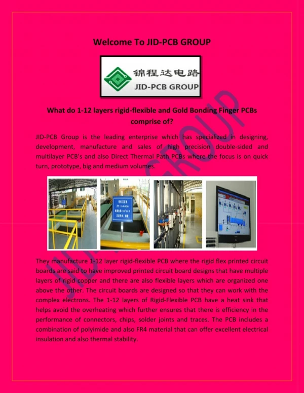
<br>High Quality PCB Co., Limited is a leading of PCB(Printed Circuit Board) Manufacturer in China since 1995. Dedicate to the technologies innovation, being engaged in IC Substrates, High-Density Interconnect PCB, Multi-layer PCB, Rigid Flexible PCB, Flexible, Radiofrequency PCB. Both prototypes and mass production projects are available for High Quality PCB.

plating gold PCB
E N D
Presentation Transcript
WELCOME TO efpcb.com W: www.efpcb.com T: +86-755-23724206 E: sales@efpcb.com
Micro Via PCB, Multilayer PCB Name: micro via PCB, multilayer PCB Layer count: 6 HDI PCBMaterial: FR4 , 0.6mm, high TG, 0.5 OZ for all layerMinimum tack: 3 milMinimum space(gap): 3 milMinimum hole: 0.15mmSurface finished: ENIGPanel size: 220*268mm/16up Application: Communications deviseCharacteristics: high density interconnect PCB, via on pad(plug with resin, copper capping), high TG, thin core 3mil thickness Rigid Flexible PCB, Rigid Flex Printed Circuit Board Part No.: E0415060179A Layer count: 4 layerMaterial: FR4, 1.6mm, high TG +1mil PI, 1 OZ for all layerMinimum tack: 5 milMinimum space(gap): 5 milMinimum hole: 0.25mmSurface finished: ENIG Panel size: 228*328mm/8up Application: Telecommunication equipment
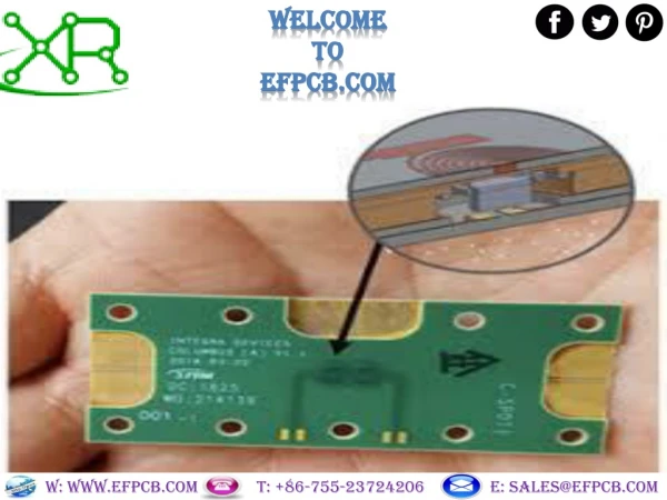
A Printed Circuit Board or PCB is now being used in various electronic appliances. However, the PCB designing is the most vital part that signifies how the last item will look like and work. An effective PCB configuration is one that backings the working of the gadget inside which it is held up. Talking about PCB assembly and manufacturing, there are various processes that include in the printing of PCB prototypes such as component designators, switch settings, and test points. These are the most crucial elements at the time of PCB’s assembling, testing, and servicing. Along with that, there are more subtle elements that go into this, including gold finger PCB. A brief description of gold finger PCBs: In general, the Gold finger is the gold-plated connectors that are on the edges of the printed circuit board model. They are like fingers in that they are long and tight. gold finger PCB is to protect the printed circuit board models from wear and tear as gold finger parts will be connected and out as often as possible.
The requirement for the gold finger: • The separate between gold finger and layout ought to be 1.0mm. • The thickness of sheets must be 1.0 or above . • The separation of gold finger parts must be at less 30mm. • As for the sloping of gold better, manufacturing plant can just do 30° angling. The use of gold fingers: • They are flexible and there are a few employment of them dependent on their proposed reason. • It offers associations for system exchange data. • It attaches superior adaptors. • It connects distinctive gadgets to the board. • It can be utilized as sound connectors.
When it comes to the design of plating gold PCB, there are certain guidelines that should be considered::- • No plated through openings can be incorporated anyplace close to the gold fingers. • No patch veil or screen printing can be incorporated close to the gold fingers. • The gold fingers ought to dependably be put confronting outward of the board's inside Above all, there are various companies available online provide the best quality of gold finger PCBs and they also offer backplane board at the best price. Contact them to find the best suppliers.
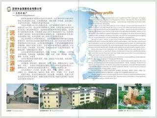
High Quality PCB Co., Limited Office address: ShajingTown,BaoanDistrict ,Shenzhen ,518000, China Plant 1 address: Building 5-6, Fu Qiao 3rd Industrial Zone, Bao' an, Shenzhen, Guangdong, China. Plant 2 address: Zhuhai, Guangdong,China Plant 3 address: Dongguan, Guangdong, China TEL: +86-755-23724206 Skype: shawnwang2006 Email: sales@efpcb.com http://efpcb.com/