Reconfigurable Communication System Design
320 likes | 427 Vues
Explore the design methodology and simulation results of a QPSK communication system on FPGAs, including carrier recovery, signal shaping, and hardware testing.

Reconfigurable Communication System Design
E N D
Presentation Transcript
Reconfigurable Communication System Design Anthony Gaught Advisors: Dr. In Soo Ahn and Dr. Yufeng Lu Department of Electrical and Computer Engineering Bradley University, Peoria, Illinois May 7, 2013
Outline • Motivation • Project Goals • Introduction to QPSK • System Block Diagram • Design Methodology • Simulation Results • Hardware Results • Conclusions • References
Motivation • In cellular systems, different data rates are achieved by adjusting modulation and channel coding schemes. A reconfigurable system can meet the ever-increasing demands and reduce the cost of system. • Quadrature Phase Shift Keying (QPSK) is one of the modulation methods adopted in various wireless communication standards. • Different design tools are available to design and implement communication systems. Each has its own advantages and disadvantages.
Project Goals • Design a complete QPSK communication system on Field Programmable Gate Arrays(FPGAs) using hardware description language (HDL). • Implement a carrier recovery circuit and a digital phase locked loop to resolve carrier offset in the receiver. • Design and verify the communication system in an efficient way. • Construct the system with hardware-efficient modules which can be reusable and expandable with additional features in the future.
QPSK Constellation Plot • s(t) = I(t)cos(2πfct) – Q(t)sin(2πfct) • Each symbol represents two bits of data. • I and Q bits are determined based on the phase of the received symbol.
Carrier Recovery • A small frequency offset is present between the transmitter and receiver. • Coherent detection is achieved by using a phase locked loop (PLL). • A direct digital synthesizer creates coherent sine and cosine carriers. • Carrier signals from the transmitter and receiver need to be synchronized in order to correctly demodulate the received data.
Calculating Phase Error • Ihat(n) and Qhat(n) are the outputs from decimators. • I(n) and Q(n) are estimated hard-decoded data. • Φ is the phase error. • Phase error is used to adjust the frequency and phase of the local oscillator.
Proportional and Integral (PI) Control • PI control provides a means to control bandwidth and dampening factor. • By optimizing Kp and Ki fast locking time and reduced jitter can be achieved. • Bandwidth is chosen first and other parameters are derived using the equations to the left.
Phase Ambiguity • Static phase error can occur at integer multiples of 90 degrees • Four possible states as seen on the constellation grid • Can be corrected by differential coding or transmitting a known sequence to synchronize the system
Signal Shaping • Raised cosine filter • Reduces inter-symbol interference (ISI) • Improves bandwidth
System Specifications • Specificationone FPGAtwo FPGAs • System clock frequency 50 MHz 50 MHz • Carrier Frequency 12.5 MHz 184 KHz • Symbol Rate 6.25 Msps 91.9 Ksps • Data Rate 12.5 Mbps 184 Kbps • Maximum Carrier Offset 1 KHz 14.7 Hz
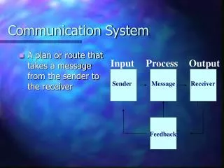
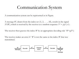
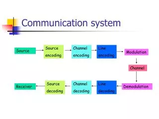
System Block Diagram • The QPSK signal, s(t), includes in-phase component, I(t), and quadrature component, Q(t). • r(t) = s(t) + n(t) where n(t) is noise.
Simulation Results • VHDL simulation results plotted are against the SIMULINK model results using MATLAB. • Fixed point representation is used throughout the HDL design.
Pulse Shaping Filter Outputs • Data type: FIX 12_11
Modulated Signal s(n) • Data type: FIX 12_11
Demodulator Outputs • Data type: FIX 12_11
Decimator Outputs • Data type: FIX 16_15
SIMULINK VS. VHDL (Ihat & Qhat) • Error on Ihat and Qhat due to fixed point representation and truncation • Ihat Mean square error = 5.44 x 10⁻⁵ • Qhat Mean square error = 5.68 x 10⁻⁵
Carrier Recovery Output • Data type: FIX 32_31 Frequency offset = 500 Hz Mean square error = 1.86 x 10⁻¹¹
Transmitted vs. Received Data • Data type: FIX 2_0
Hardware Results • The design is implemented on Spartan 3E Boards. • P-mod DA2 and P-mod AD1 modules are used transmit the signal between FPGAs. • Signals of interest are displayed on an oscilloscope.
Transmitted Data • Constellation plot for the transmitted data
Received Data • Constellation plot for the received data • Transmitter and receiver on the same FPGA • s(n) is an internal digital signal. Frequency offset < 1 KHz Frequency offset > 1 KHz
Received Data Cont. • Constellation plot for the received data • Transmitter and receiver on separate FPGAs • s(t) is an external analog signal. Frequency offset < 14.7 Hz Frequency offset > 14.7 Hz
Transmitted vs. Received Data • Data type: FIX 2_0 (From top down) • Transmitted data • Received data on the same FPGA • Received data on separate FPGAs
Observed Phase Ambiguity (From top down) • It • Qt • Ir • Qr
Observed Phase Ambiguity Cont. (From top down) • It • Qt • Ir • Qr
Possible Future Features • Correct for phase ambiguity • Wireless transmission of the modulated signal • Implementation of other modulation schemes such as higher order PSK, quadrature amplitude modulation (QAM) or others
Conclusions • In this project, a reconfigurable QPSK communication system has been designed using HDL. • The system has been implemented on low-cost Xilinx Spartan3E boards. • An efficient verification flow has been applied to the design. • Carrier recovery circuit and digital phase locked loop are used to resolve carrier offset which is essential for decoding of the transmitted data.
References • Anton Rodriguez, and Michael Mensinger Jr., “Software-defined Radio using Xilinx”, Senior Project Report, Department of Electrical and Computer Engineering, Bradley University, Peoria Illinois, May 2011. • Anthony Gaught, Alexander Norton, and Christopher Brady., “FPGA-based 16 QAM communication system”, Digilent design contest Report, Department of Electrical and Computer Engineering, Bradley University, Peoria Illinois, April 2012. • Leon Couch, “Digital and analog communication systems”, 8th edition, Boston: Pearson, 2013.