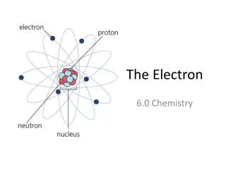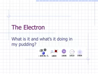
The Electron
The Electron. By a Gentleman. Insulators and Conductors. -. +. Conduction. All conduction is due to the movement of free electrons. I’m free. In a Semiconductor the electrons are fixed until they receive a little energy. The Silicon, Si, Atom.

The Electron
E N D
Presentation Transcript
The Electron By a Gentleman
- + Conduction • All conduction is due to the movement of free electrons. I’m free In a Semiconductor the electrons are fixed until they receive a little energy
The Silicon, Si, Atom Silicon has a valency of 4 i.e. 4 electrons in its outer shell Each silicon atom shares its 4 outer electrons with 4 neighbouring atoms These shared electrons – bonds – are shown as horizontal and vertical lines between the atoms This picture shows the shared electrons
Intrinsic Semiconductors I’m free • Conductivity half way between a conductor and an insulator • Crystals of pure Silica • A photon releases an electron that now can carry current
Intrinsic Semiconductors • A photon releases an electron that now can carry current
Heating Silicon We have seen that, in silicon, heat releases electrons from their bonds… This creates electron-hole pairs which are then available for conduction
Intrinsic Conduction If more heat is applies the process continues… More heat… More current… Less resistance… The silicon is acting as a thermistor Its resistance decreases with temperature Slide 8
The Thermistor • Thermistors are used to measure temperature • They are used to turn devices on, or off, as temperature changes • They are also used in fire-warning or frost-warning circuits Thermistor Symbol
Light Dependent Resistor (LDR) • The LDR is very similar to the thermistor – but uses light energy instead of heat energy • When dark its resistance is high • As light falls on it, the energy releases electron-hole pairs • They are then free for conduction • Thus, its resistance is reduced LDR Symbol
Resistance Resistance Amount of light Temperature Two semiconductor devices 1) Light dependant resistor – resistance DECREASES when light intensity INCREASES 2) Thermistor – resistance DECREASES when temperature INCREASES
Digital thermometer 10°C Ω Water Thermistor Glycerol Heat source THE VARIATION OF THE RESISTANCE OF A THERMISTOR WITH TEMPERATURE
Method 1. Set up the apparatus as shown. 2. Use the thermometer to note the temperature of the glycerol and thermistor. 3. Record the resistance of the thermistor using the ohmmeter. 4. Heat the beaker. 5. For each 10 C rise in temperature, record the resistance and the temperature using the ohmmeter and the thermometer. 6. Plot a graph of resistance against temperature and join the points in a smooth, continuous curve.
Precautions • Heat the water slowly so temperature does not rise at end of experiment • Wait until glycerol is the same temperature as water before taking a reading.
Extrinsic Semiconductors • Doping is adding an element of different valency to increase conductivity of semiconductor
Extrinsic Semiconductors • P-type have more holes (Add Group3)
The Boron Atom Boron is number 5 in the periodic table It has 5 protons and 5 electrons – 3 of these electrons are in its outer shell
Extrinsic Semiconductors • N-type have more electrons (Add Group5)
The Phosphorus Atom Phosphorus is number 15 in the periodic table It has 15 protons and 15 electrons–5 of these electrons are in its outer shell
Extrinsic Conduction – p-type silicon A current will flow – this time carried by positive holes Note: The positive holes move towards the negative terminal
Junction Diode • Two types grown on the same crystal P-type N-type
Junction Diode • Near the junction some electrons from the ‘N’ fill the holes in the ‘P’ crystal. P-type N-type
This barrier is called the DEPLETION LAYER Junction Diode • This creates area in the middle where there are no carriers so no conduction P-type N-type
Junction Diode • When the diode is in FORWARD BIAS the depletion layer disappears. The diode conducts. - + P-type N-type
Junction Diode • When the diode is in REVERSE BIAS the depletion layer increases. The diode acts as a barrier or insulator. - + P-type N-type
2009 Question 12(b)[Higher Level] • A semiconductor diode is formed when small quantities of phosphorus and boron are added to adjacent layers of a crystal of silicon to increase its conduction. • Explain how the presence of phosphorus and boron makes the silicon a better conductor. • What happens at the boundary of the two adjacent layers? • Describe what happens at the boundary when the semiconductor diode is forward biased • Describe what happens at the boundary when the semiconductor diode is reverse biased. • Give a use of a semiconductor diode.
Homework • 2004 HL Q12(d)
0.6 V The p-n Junction – no potential As the p-type has gained electrons – it is left with an overall negative charge… As the n-type has lost electrons – it is left with an overall positive charge… Therefore there is a voltage across the junction – the junction voltage – for silicon this is approximately 0.6 V
The Reverse Biased P-N Junction Take a p-n junction Apply a voltage across it with the p-type negative n-type positive Close the switch The voltage sets up an electric field throughout the junction The junction is said to be reverse – biased
Thus, the depletion layer ( INSULATOR ) is widened and no current flows through thep-n junction The Reverse Biased P-N Junction Negative electrons in the n-type feel an attractive force which pulls them away from the depletion layer Positive holes in the p-type also experience an attractive force which pulls them away from the depletion layer
The Forward Biased P-N Junction Take a p-n junction Apply a voltage across it with the p-type postitive n-type negative Close the switch The voltage sets up an electric field throughout the junction The junction is said to be forward – biased
The Forward Biased P-N Junction Negative electrons in the n-type feel a repulsive force which pushes them into the depletion layer Positive holes in the p-type also experience a repulsive force which pushes them into the depletion layer Therefore, the depletion layer is eliminated and a current flows through the p-n junction
The Forward Biased P-N Junction At the junction electrons fill holes Both disappear as they are no longer free for conduction They are replenished by the external cell and current flows This continues as long as the external voltage is greater than the junction voltage i.e. 0.6 V
The Forward Biased P-N Junction If we apply a higher voltage… The electrons feel a greater force and move faster The current will be greater and will look like this…. The arrow shows the direction in which it conducts current The p-n junction is called a DIODE and is represented by the symbol…
Diode as Valve • Only allows current in one direction Forward Bias Reverse Bias
LED • An LED (Light Emitting Diode) works in the same way. We use it for pin lights. Forward Bias Reverse Bias
Characteristic Curve - Diode I/A In reverse Bias No conduction V/v Junction Voltage (0.6V) Must be Overcome before Conduction starts
VARIATION OF CURRENT (I) WITH P.D. (V) mA Diode in forward bias + 6 V - V
VARIATION OF CURRENT (I) WITH P.D. (V) A Diode in Reverse bias + 6 V - V
Rectifier • Uses this to turn AC to DC Mains Resistor • This is called half wave rectification
Rectifier • We use a capacitor to smooth the signal to get something more like DC
Amplification • On 16 December 1947 William Shockley, John Bardeen and Walter Brattain built the first practical transistor at Bell Labs • Despite hardly talking to each other.
Transistors • Small changes in the input signal greatly changes the size of the depletion layer The current increases if the D.P. is small 3A 1A 10mA 30mA
Signal Amplification • So small changes in input signal create large charges in output.
Thermionic Emission • Electrons (as named by G. Stoney) leaving the surface of a hot metal e- e- e- e- e- Hot Metal
A N O D E e- High Voltage Cathode Rays (Really Electrons) • First we heat the cathode to make the electrons jump off by Thermionic Emission We can use a high voltage to accelerate the electrons to form a stream C A T H O D E e-
A N O D E e- 1v Electron Energy Units • We calculate the energy of each electron first in electron volts. The energy gained when an electron crosses a potential difference of 1Volt. Energy Gained = 1 eV C A T H O D E e-
A N O D E e- 2000v Electron Energy • We calculate the energy of each electron first in electron volts Energy Gained = 2000eV C A T H O D E e-
A N O D E e- 2000v Electron Energy • Then we convert this to joules ( Charge on the electron = e = 1.6x10⁻¹⁹ C) Energy Gained = e.V = 1.6x10⁻¹⁹ . 2000 = 3.2x10⁻¹⁶ Joules C A T H O D E e-
A N O D E e- 2000v Electron Velocity • All the energy on an electron must be kinetic energy. Energy Gained = 3.2x10-16 = 0.5mv2 electron mass = 9.1 × 10⁻³¹ kg C A T H O D E e-